Growth and Characterization of Jet Nebulizer Spray Deposited N-type WO3 Thin films for Junction Diode Application
K. Shanmugasundaram1, P. Thirunavukkarasu1, M. Ramamurthy2, M. Balaji2 and J. Chandrasekaran2
1Department of Electronics, Sri Ramakrishna Mission Vidyalaya College of Arts and Science, Coimbatore 641020, Tamil Nadu, India.
2Department of Physics, Sri Ramakrishna Mission Vidyalaya College of Arts and Science, Coimbatore 641020, Tamil Nadu, India.
Corresponding Author E-mail: iruarasu@yahoo.co.in
DOI : http://dx.doi.org/10.13005/ojc/330542
Tungsten Trioxide Thin Films; JNSP Technique; P-N Junction Diode; Ideality Factor; Barrier Height
Download this article as:| Copy the following to cite this article: Shanmugasundaram K, Thirunavukkarasu P, Ramamurthy M, Balaji M, Chandrasekaran J. Growth and Characterization of Jet Nebulizer Spray Deposited N-type WO3 Thin films for Junction Diode Application. Orient J Chem 2017;33(5). |
| Copy the following to cite this URL: Shanmugasundaram K, Thirunavukkarasu P, Ramamurthy M, Balaji M, Chandrasekaran J. Growth and Characterization of Jet Nebulizer Spray Deposited N-type WO3 Thin films for Junction Diode Application. Orient J Chem 2017;33(5). Available from: http://www.orientjchem.org/?p=37959 |
Introduction
Transition Metal Oxides (TMOs) have attracted substantial interest owing to their potential applications such as sensors, solar cells, photocatalysis and electrochromic devices [1-5]. ZnO, TiO2, SnO2, MoO3 and WO3 are the most standard semiconductor metal oxides used in the optoelectronic devices. Among them, tungsten trioxide (WO3) is used in many electronic devices because of its tunable properties of chemical composition, surface morphological, optical absorption in visible range and high thermal stability [6, 7]. Several preparation techniques have been used to deposit tungsten oxide thin films, including sol-gel, spray pyrolysis, chemical vapour deposition, RF sputtering, plasma evaporation, electrodeposition, etc [8-18]. In fact, spray pyrolysis is one of the most versatile techniques to deposit oxide films, allowing the control of many properties of the films by changing the preparation parameters of the technique. It is very simple, economical and a suitable method for large area coating for many semiconducting thin films.
The aim of this work is to prepare WO3 thin films using modified spray technique of jet nebulizer spray pyrolysis (JNSP) technique [19-21]. The prepared WO3 films were characterized by structural, optical and electrical properties. Finally, n-WO3/p-Si junction diode parameters were observed using the current-voltage (I-V) measurements.
Experimental Details
Preparation of WO3 thin films
The precursor solution was prepared with different mole concentrations of 0.10, 0.15, 0.20 and 0.25 M of tungsten (VI) chloride (WCl6) and de-ionized water. WO3 thin films were coated on well cleaned glass substrates (2 x 2 cm) under three variable conditions to optimize deposition parameters as follows (i) Initially, the WO3 thin films were prepared by varying the volume of solution (3, 5, 7 and 9 ml) with constant substrate temperature of 500°C and 0.10 mole concentration for optimizing the volume level of the solution. (ii) Then by varying the mole concentration (0.05, 0.10, 0.15 and 0.20 M) with fixed 500°C substrate temperature and volume of solution as 5ml, for optimizing the mole concentration, (iii) Finally, WO3 thin films were prepared by varying the substrate temperatures (400, 450, 500 and 550°C) with optimized molarity as 0.2 M and volume level as 5 ml and the temperature is optimized.
Fabrication of n-WO3/p-Si Junction Diode
Prior to the fabrication of junction diode, silicon (Si) wafer is cleaned well by Piranha solution (3:1 of H2SO4:H2O2) to remove impurities like organic residues, dust and grease. Next to remove the native oxides from the Si wafer by H2O: HF (10:1) solution. The precursor solution of 20 ml with 0.20 M was coated on p-type Si wafer (1 x 1 cm) at 500°C substrate temperature to form the n-WO3/ p-Si junction diode. After the formation of n-WO3/ p-Si diode, the silver (Ag) paste (ELTECK Corporation) was applied on the both surfaces of the junction for better electrical contacts. The Ag applied sample is dried at ambient condition for about 6 hr. The current- voltage (I-V) measurement under dark and light illumination (650 W halogen lamps) was carried out using Keithley Electrometer (6517B).
Characterization Technique
The X-ray diffractometer (XRD)(XPERT-PRO) with CuKα1 radiation of wavelength 1.5406 Å at a generator setting of 30 mA and 40 KV in the 2θ range from 20° to 70° was used to obtain the structure of the WO3 thin films. The surface morphology of the films were analyzed by the scanning electron microscope (SEM) (JEOL/EOJSM-6390). The presence of elements (W and O) was confirmed by the energy dispersive analysis from X-ray spectroscopy (EDAX) (BRUKER). The UV-visible spectrophotometer (Perkin Elmer Lambda 35) showed the optical properties in the wavelength range from 300 to 900 nm. DC electrical properties and n-WO3/p-Si junction diode characterizations was measured using Keithley Electrometer (6517-B).
Results and Discussion
Xrd Analysis
The as-deposited WO3 thin films have been characterized by XRD analysis. Figure 1a shows the XRD patterns of film deposited at different volume of solution from 3 to 9 ml with constant substrate temperature and mole concentration as 500°C and 0.10 M respectively. It shows that the films are polycrystalline. It also found that the deposited films at 3, 5, 7 and 9 ml are well crystallized and having monoclinic structure with major orientation along (0 2 2) plane. The preferred orientation remains along (0 2 2) plane for all films. The diffraction an angle (2θ in degree) with corresponding hkl planes coincides with JCPDS values (Card no. 83-0950) and indicates monoclinic structure. Figure 1b shows the XRD pattern of WO3 for different mole concentrations 0.05, 0.10, 0.15 and 0.20 M with constant volume 5 ml and substrate temperature 500°C. The intensity of the diffraction peaks increases with increasing mole concentration from 0.05 to 0.20 M. The diffraction peaks confirm the monoclinic structure. Figure 1c elucidates the XRD pattern of WO3 for different substrate temperature from 400°C to 550°C for fixed 0.20 M and 5 ml. Figure 1c reveals that the crystallinity increases as increasing the substrate temperature till 500°C and then decreases. It also confirms the monoclinic structure with preferred orientations of (0 2 2) planes
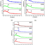 |
Figure 1: XRD patterns for different (a) volume concentrations, (b) mole concentrations and (c) substrate temperatures. |
The micro structural properties of crystallite size (D) and micro strain (ε) of WO3 thin films for the preferred orientation of (0 2 2) were calculated by the following relations (1, 2) [20, 21]

where k is the shape factor (k=0.94), λ is the wavelength of the X-ray radiation, θ is diffraction angle and β is the full width at half maximum.
Table 1: Micro structural properties for different volume concentrations
|
Volume variation (ml) |
FWHM (Radians) |
Crystallite size (D) nm |
Micro strain (ε) (x 10-3 lines-2 m-4) |
|
3 |
0.0026 |
45.73 |
0.7887 |
|
5 |
0.0023 |
46.45 |
0.7567 |
|
7 |
0.0024 |
45.38 |
0.7672 |
|
9 |
0.0027 |
44.40 |
0.7856 |
Table 2: Micro structural properties for different mole concentrations
|
Molarity Variation (M) |
FWHM (Radians) |
Crystallite size (D) nm |
Micro strain (ε) (x 10-3 lines-2 m-4) |
|
0.05 (2 0 2) |
0.0128 |
43.75 |
0.8056 |
|
0.01 (2 0 2) |
0.0115 |
44.70 |
0.7886 |
|
0.15 (2 0 2) |
0.0108 |
49.40 |
0.7556 |
|
0.20 (0 2 2) |
0.0085 |
52.22 |
0.7086 |
Table 3: Micro structural properties for different substrate temperature
|
Substrate Temperature (°C) |
FWHM (Radians) |
Crystallite size (D) nm |
Micro strain (ε) (x 10-3 lines-2 m-4) |
|
500 |
0.0037 |
53.45 |
0.6980 |
|
550 |
0.0033 |
44.03 |
0.7878 |
Table 1 illustrates the maximum crystallite size and minimum microstrain values for preferred orientation of (0 2 2) plane as 46.73 nm and 0.7887 x 10⁻³lines-2 m-4 (5 ml of volume). By varying mole concentration, the preferred orientation plane (2 0 2) changed to (0 2 2) for (Table 2) and maximum crystallite size and minimum microstrain values of 52.22 nm and 0.7086 x 10⁻³ lines-2 m-4 for 0.20 M concentration were obtained. From varying substrate temperature result, the preferred orientation of (0 2 2) plane was not obtained for 400 and 450°C owing to poor crystallinity in low temperatures. The substrate temperature of 500 and 550°C results the good crystalline nature and reveals the maximum crystallite size and minimum microstrain of 53.45 nm and 0.7878 x 10⁻³ lines-2 m-4 for the substrate temperature of 500°C (Table 3). The tables imply the variation of D and ε of WO3 films for various volumes of solution, mole concentrations and substrate temperatures. The results revealed that the 5 ml of volume, 0.20 M of concentration and 500°C of substrate temperature provide good crystalline nature of deposited films in the present study using JNSP technique.
SEM and EDAX Analysis
The surface morphological changes of WO3 films for various volume of solution, mole concentrations and substrate temperatures are shown in Figure 2, 3 and 4. In Figure 2a&b, the closely packed sub-microsized and irregular shaped grains were observed for 3 and 5 ml of volume. When the volume of the solution is increased, the large variations in surface with randomly oriented sub-microsized rectangular shaped grains were observed (Figure 2c&d).
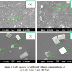 |
Figure 2: SEM images for different volume concentrations of (a) 3, (b) 5, (c) 7 and (d) 9 ml. Click here to View figure |
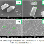 |
Figure 3: SEM images for different mole concentrations of (a) 0.05, (b) 0.10, (c) 0.15and (d) 0.20 M. Click here to View figure |
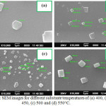 |
Figure 4: SEM images for different substrate temperatures of (a) 400, (b) 450, (c) 500 and (d) 550°C. Click here to View figure |
Figure 3a-d shows the surface morphology of different mole concentrations of WO3 films. From the images its shows the randomly oriented sub-microsized morphological results, which are similar to Figure 2. The SEM images of WO3 thin films of different substrate temperatures 400 to 550°C are shown in Figure 4a-d. It observes that the increase in substrate temperature grains are arranged sub-microsized rectangular and square shaped structures of WO3 films.
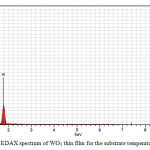 |
Figure 5: EDAX spectrum of WO3 thin film for the substrate temperature of 500°C. Click here to View figure |
Figure 5 depicts the EDAX spectrum of WO3thin films deposited at a substrate temperature of 500°C. It showed that the presence of elements W and O is confirmed.
UV-vis Spectra
Figure 6a illuminates the variation of transmittance with wavelength for the WO3 thin films deposited at different substrate temperatures 400, 450, 500 and 550ºC. The average transmission in the visible region has been found to vary from 70 to 85% depending upon the substrate temperature. As increase in transmission is observed with increase in deposition temperature. At relatively lower temperatures less than 500ºC, lower transmission is observed due to which is the formation of uneven films and incomplete decomposition of the sprayed droplets. The variation of transmittance owes to increase in packing density and decrease in thickness of the film which is due to shrinking of spray droplets [22].
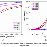 |
Figure 6a: Transmittance spectra and (b) Band gap energy for different substrate temperatures Click here to View figure |
From the UV-vis spectra, the band gap energy (Eg) for WO3 films is calculated using equation (3) [23],
αhυ2 = B(hυ-Eg) (3)
where α is the absorption co-efficient, hυ is the photon energy, B is the constant and Eg is the band gap energy. Figure 6b displays the plot of (αhυ)2 vs. (hυ) for the WO3 thin films deposited at different substrate temperatures. It can be seen that the plots are linear in the region of strong absorption i.e. near fundamental absorption edge. Extrapolation of the linear portion to (αhυ)2 is equal to zero gives the direct band gap energy of the films are found to vary as 2.63, 2.58, 3.86 and 3.80 eV for different substrate temperatures 400, 450, 500 and 550ºC respectively. The maximum band gap energy 3.86 eV [24] is obtained for the substrate temperature 500ºC. This high value of band gap confirms the surface smoothness and uniformity of deposited thin films. Also a shift in band gap to higher energies is attributed to increased carrier density and to the change in crystallinity of the films with temperature [25].
DC Electrical Properties
The current and voltage (I-V) measurements of WO3 thin films prepared for various volume of solution, mole concentrations and substrate temperatures were taken at room temperature using Keithley Electrometer through two probe. The current values were measured for different applied voltages from 10 to 100 V. The DC conductivity (σ) for WO3 films was calculated using the given equation (4) [20,21],
![]()
where I is current, V is applied potential, d is inter-probe distance and A is cross-sectional area of the film.
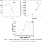 |
Figure 7: Average conductivity values for different (a) voume concentrations, (b)mole concentrations and (c) substrate temperatures. Click here to View figure |
Figure 7a shows the variation of conductivity with different volume of solution of deposited WO3 thin films. It shows that the average conductivity values are 3.443 x 10⁻⁸, 5.133 x 10⁻⁸, 4.395 x 10⁻⁹ and 3.699 x 10⁻⁹ S/cm for volume of solution from 3 to 9 ml respectively. Also shows that the conductivity value increased up to 5 ml and then decreases. Figure 7b shows the average conductivity of deposited WO3 thin films at different mole concentrations of 0.05, 0.10, 0.15 and 0.20 M. The graph shows that the maximum conductivity 1.631 x 10⁻⁸ S/cm for the film deposited at 0.20 M. The variation of average conductivity with different substrate temperature of deposited WO3 thin films as shown in Figure 7c. It observed that the average conductivity values of WO3 films are 4.349 x 10⁻⁹, 5.726 x 10⁻⁹, 1.201 x 10⁻⁸ and 1.130 x 10⁻⁸ S/cm. Also shows that the film deposited at substrate temperature of 500ºC have the maximum value of conductivity. The variations of values in conductivity may be due to the oxygen vacancies in the prepared WO3 thin films [21, 26-28]. The increasing of conductivity with the substrate temperature owing to the variation in morphology and the increasing of grain size, which reduced the lattice dislocations and imperfections of the W-O matrix. This phenomenon decreases the grain boundary volume associated with flow of charge carriers [29].
I-V Characterization of n-WO3/p-Si Junction Diode
The junction formation of the P-N diode is carried out by the n-type WO3 and p-type Si substrate. The P-N junction diode of n-WO3/p-Si was prepared by the optimized conditions of volume of solution (5 ml), mole concentration (0.20 M) and substrate temperature (500ºC) by JNSP technique. The prepared n-WO3/p-Si junction diode parameters of ideality factor (n) and barrier height (Φb) were measured under darkness and illumination of light (halogen + metal halide-100 mW/cm2) [20]. The reverse to forward bias current measurement is taken for the applied voltage of -4 to +4 V. Figure 8 shows the I-V characteristics of n-WO3/p-Si junction diode under dark and illumination. The n-WO3/p-Si junction diode exhibits a good rectifying nature in dark and under illumination.
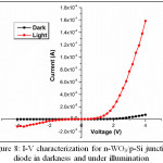 |
Figure 8: I-V characterization for n-WO3/p-Si junction diode in darkness and under illumination Click here to View figure |
Figure 9 illustrates the semi-log plot of the current density (ln J) versus applied voltage (V). The diode parameters of ideality factor (n) and barrier height (Φb) are calculated from the forward bias J-V plot. These parameters provide an information about the charge transport mechanism of the p-n junction interface and the electrode contact with the tungsten oxide layer. Using the thermionic emission (TE) equations, the current density of the n-WO3/p-Si junction diode was calculated as follows (5) [21,30],
![]()
where Jo is reverse saturation current density, q is charge of electron, V is applied potential, n is ideality factor, K is Boltzmann constant and T is absolute temperature.
Using equation (5) for V ≥ 3kT/q, n and Jo values were obtained from the slope and interception of semi-log forward bias J-V plot. Thus, n and Φb were calculated by the following equations (6,7) [21,30],
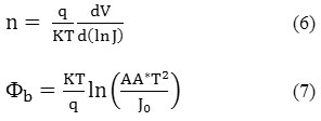
where A is the active area of prepared diode and A* is the Richardson constant.
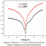 |
Figure 9: Plots ln J vs. V for n-WO3/p-Si junction diode in darkness and under illumination Click here to View figure |
The n and Φb values under darkness is obtained as 5.8 and 0.80 eV and under light illumination as 3.9 and 0.81 eV. The n value is unity (i.e., n = 1) for an ideal P-N diode but in the present work, the n values are obtained as more than unity. The obtained result of n value is comparable to the reported value of 3.5, for a reactive magnetron sputtering deposited Ag/n-WO3/p-Si Schottky diode [31]. The results suggest that the non-ideal behavior of prepared n-WO3/p-Si junction diode which may be owing to the presence of an interfacial thin native oxide layer (SiO2) and barrier in-homogeneities [20,21,30].It may also be owing to series resistance and nonlinear metal-semiconductor contact [20,32]. Another reasons may be the abnormalities of the inorganic film thickness and non-uniformity of the interfacial charges [20,33].
Conclusion
The WO3 thin films have been prepared using JNSP technique and the conditions of volume of solution, mole concentrations and substrate temperatures were optimized. From the XRD results, it was observed that the prepared WO3 film has monoclinic structure and also has the maximum crystallite size as 46.45, 52.22 and 53.45 nm for 5 ml of volume, 0.20 M of molarity and 500ºC of substrate temperature respectively. The surface morphological variations of sub-microsized grains of WO3 were displayed by SEM analysis for different volume, molarity and substrate temperatures and the presence of elements such as W and O were confirmed by EDAX results. UV-vis for various substrate temperatures was observed and it showed the maximum transmission value and maximum band gap energy of 3.86 eV for the substrate temperature of 500ºC. The DC electrical conductivity reveals that the 5 ml of volume, 0.20 M of molarityand 500ºC of substrate temperature has maximum conductivity values of 5.133×10-8,1.631×10-8and 1.201×10⁻⁸ S/cm. Based on the optimized volume (5ml), molarity (0.20 M) and substrate temperature (500ºC), the n-WO3/p-Si junction diode was prepared using JNSP technique. The diode parameters of ideality factor (n) values were measured as 5.8 in darkness and under illumination as 3.9.The photoconduction nature of the prepared n-WO3/p-Si junction diode will be endorsed for photo-detector application.
References
- Gao, P.; Ji, H.; Zhou, Y.; Li, X. Thin Solid Films 2012, 520, 3100-3106.
CrossRef - Zheng, H.; Ou J.Z.; Strano, M.S.; Kaner, R.B.; Mitchell, A.; Kalantar-zadeh, K. Adv. Funct. Mater. 2011, 21, 2175-2196.
CrossRef - Jiao, Z.; Wang, J.; Ke, L.; Sun, X.W.; Demir, H.V. ACS Appl. Mater. Interfaces 2011, 3, 229-236.
CrossRef - Deepa, M.; Saxena, T.K.; Singh, D.P.; Sood, K.N.; Agnihotry, S.A. Electrochim. Acta 2006, 51, 1974-1989.
CrossRef - Youn, J.H; Baek, S.J.; Kim, H.P.; Nam, D.H.; Lee, Y.; Leeb, J.G.; Jang, J. J. Mater. Chem. C 2013, 1, 3250-3254.
CrossRef - Hyett, G.; Blackman, C.S.; Parkin, I.P. Faraday Discuss. 2007, 136, 329-343.
CrossRef - Jayachandran, M.; Vijayalakshmi, R.; Ravindran, V.; Sanjeeviraja, C. Trans. SAEST 2005, 40, 42-61.
- Badilescu, S.; Ashrit, P.V. Solid State Ionics 2003, 158, 187-197.
CrossRef - Enesca, A.; Duta, A. Phys. Stat. Sol. (c) 2008, 5, 3499-3502.
CrossRef - Palgrave, R.G.; Parkin, I.P. J. Mater. Chem. 2004, 14, 2864-2867.
CrossRef - Karuppasamy, A. Appl. Surf. Sci. 2013, 282, 77-83.
CrossRef - Tseng, C.J.; Wang, C.H.; Cheng, K.W. Sol. Energy Mater. Sol. Cells 2012, 96, 33-42.
CrossRef - Intyushin, E.B.; Novikov, V.A. Thin Solid Films 2008, 516, 4194-4200.
CrossRef - Koebel, M.M.; Nadargi, D.Y.; Cadena, G.J.; Romanyuk, Y.E. ACS Appl. Mater. Interfaces, 2012, 4, 2464-2473.
CrossRef - Li, W.; Liu, C.; Yang, Y.; Li, J.; Chen, Q.; Liu, F. Mater, Lett. 2012, 84, 41-43.
CrossRef - Zhang, C.; Debliquy, M.; Boudiba, A.; Liao, H.; Coddet, C. Sens. Actuators B 2010, 144, 280-288.
CrossRef - Isik, D.; Ak, M.; Durucan, C. Thin Solid Films 2009, 518, 104-111.
CrossRef - Kharade, R.R.; Patil, K.R.; Patil, P.S.; Bhosale, P.N. Mater. Research Bullet. 2012 doi:10.1016/j.materresbull.2012.03.025.
CrossRef - Sethupathi, N.; Thirunavukkarasu, P.; Vidhya, V.S.; Thangamuthu, R.; Kiruthika, G.V.M.; Perumal, K.; Bajaj, H.C.; Jayachandran, M. J. Mater. Sci.: Mater. Electron. 2012, 23, 1087-1093.
CrossRef - Balaji, M.; Chandrasekaran, J.; Raja, M. Mater. Sci. Semicond. Process. 2016, 43, 104-113.
CrossRef - Balaji, M.; Chandrasekaran, J.; Raja, M.; Rajesh, S. J. Mater. Sci.: Mater. Electron. 2016, 27, 11646-11658.
CrossRef - Suresh, R.; Ponnuswamy, V.; Mariappana, R.; Senthil Kumar, N. Ceram. Int. 2014, 40, 437-445.
CrossRef - Balaji, M.; Chandrasekaran, J.; Raja, M. Optik 2016, 127, 6015-6027.
CrossRef - Sivakumar, R.; Raj, A.M.E.; Subramanian, B.; Jayachandran, M.; Trivedi, D.C.; Sanjeeviraja, C. Mater. Research Bullet. 2004, 39, 1479-1489
CrossRef - Davazoglou, D.; Leveque, G.; Donnadieu, A. Sol. Energy Mater. 1988, 17, 379-390.
CrossRef - Nirupama, V.; Chandrasekhar, M.; Radhika, P.; Sreedhar, B.; Uthanna, S. J. Optoelectron. Adv. Mater. 2009, 11, 320- 325.
- Nirupama, V.; Chandra Sekhar, M.; Subramanyam, T.K.; Uthanna, S. J. Phys.: Conf. Ser. 2010, 208, 012101(1-6).
- Sutrave, D.S.; Gothe, S.D. DAMA Int. 2015, 2, 1-6.
- Raja, M.; Chandrasekaran, J.; Balaji, M.; Janarthanan, B. Mater. Sci. Semicond. Process. 2016, 56, 145-154.
CrossRef - Raja, M.; Chandrasekaran, J.; Balaji, M. Optik 2016, 127, 11009-11019.
CrossRef - Tombak, A.; Benhaliliba, M.; Ocak, Y.S.; Kilicoglu, T. Result. Phys. 2015, 5, 314-321.
CrossRef - Wang, C.X.; Yang, G.W.; Liu, H.W.; Han, Y.H.; Luo, J.F.; Gao, C.X.; Zou, G.T. Appl. Phys. Lett. 2004, 84, 2427-2429.
CrossRef - Suresh, R.; Ponnuswamy, V.; Mariappan, R. Ceram. Int. 2015, 41, 3081-3093.
CrossRef

This work is licensed under a Creative Commons Attribution 4.0 International License.


