Enhanced Characteristics of Square-Shaped Extended Source TFET Via Silicon Carbide Polytype (3C-Sic) and A Dopant Pocket Layer
Saeid Marjani1, Saeed Khosroabadi2 and Seyed Ebrahim Hosseini1
1Department of Electrical Engineering, Ferdowsi University of Mashhad, Mashhad, Iran.
2Department of Electrical Engineering, Imam Reza International University, Mashhad, Iran.
Corresponding Author E-mail: saeid.marjani@mail.um.ac.ir
DOI : http://dx.doi.org/10.13005/ojc/330303
In this paper, for the first time, the square-shaped extended source tunneling field-effect transistor (SES TFET) by means of the silicon carbide polytype (3C-SiC) and dopant pocket layer has been presented. By inserting the silicon carbide polytype as substrate and n-type pocket in the channel at the source edge, on-current is increased by about 10 times compared with the conventional SES TFET because of the reduced losses and energy band modification imposed by the silicon carbide and pocket doping, respectively. Additionally, using calibrated simulations, the SES TFET with 3C-SiC substrate and dopant pocket layer is evaluated in terms of various radio-frequency (RF) parameters, including the gate to source capacitance, gate to drain capacitance, transconductance, channel resistance, transport time delay, cutoff and maximum oscillation frequencies. The simulation results of the SES TFET with the 3C-SiC substrate and dopant pocket layer exhibits a superior switching-state current ratio (∼1013) and a small transport time delay (about 0.15 psec) that is a hopeful candidate for conventional SES TFET.
KEYWORDS:Silicon carbide polytype (3C-SiC); Cubic zinc-blende; Transport time delay; Switching-state current ratio; Dopant pocket layer; Tunneling field-effect transistors (TFETs)
Download this article as:| Copy the following to cite this article: Marjani S, Khosroabadi S, Hosseini S. E. Enhanced Characteristics of Square-Shaped Extended Source TFET Via Silicon Carbide Polytype (3C-Sic) and A Dopant Pocket Layer. Orient J Chem 2017;33(3). |
| Copy the following to cite this URL: Marjani S, Khosroabadi S, Hosseini S. E. Enhanced Characteristics of Square-Shaped Extended Source TFET Via Silicon Carbide Polytype (3C-Sic) and A Dopant Pocket Layer. Orient J Chem 2017;33(3). Available from: http://www.orientjchem.org/?p=33695 |
Introduction
Over the past few years, silicon carbide (SiC) polytypes have been concerned as the alternative semiconductor materials for future high temperature power semiconductor devices at high frequency with reduced power losses and die size because of their large breakdown and drift velocity in saturation state; sensibly high mobility, and reasonably good thermal conductivity [1–5]. The first commercial silicon carbide devices were obtained as high power Schottky diodes in year 2001 [6].
There are many different polytypes of SiC (over 200), including cubic, hexagonal and rhombohedral variants, where they have widely ranging physical properties. They are variations of the same chemical compound that are identical in two dimensions and differ in the third (different stacking sequences). Therefore, each of them exhibit different electrical, optical and thermal properties. The Si-C bilayers atomic stacking sequences along [111] direction determine all the its polytypes, the most common amongst which are zinc-blende structure that Si and C inhabit ordered positions in a diamond structure; hexagonal (2H, 4H and 6H) or α-SiC and rhombohedral (15R) type SiC that stated to as αη-SiC, n Si-C bilayers include stack of C and Si layers in the primitive cell [2, 5,]. Due to the reduced scattering resulting from the breaking of an out-of-plane symmetry selection rule, 3C-SiC has the highest electron mobility and saturation velocity [5]. Figures 1 and 2 show the lattice structures and distribution in circumstellar 3C-SiC by means of transmission-electron-microscopy (TEM) on presolar silicon carbide in the Murchison carbonaceous chondrite [7], which is most important for this paper.
One of the promising new developments in the semiconductor transistors research is tunneling field-effect transistor (TFET) due to the its low subthreshold swing and low off-state leakage current [8–15]. Its current is based on the tunneling effect at the source to channel edge. Therefore, TFETs can overcome the supply voltage scaling issues, the 60 mV/decade subthreshold slope and power consumption limits of MOSFET devices at room temperature [16, 17]. Due to the insignificant band-to-band tunneling phenomenon in silicon TFETs, they have low on-currents that one of the major concerns in the design and fabrication of these transistors is to improve their on-current performance. On the other hand, an increase in on-current causes the RF performances of the TFETs to be enhanced. To enhance the TFET on-currents, many efforts have been made including hetero-structures [11, 16, 17], band-gap engineering [18, 20], high mobility and low band-gap materials [20, 23], high-k dielectric materials [24, 25], hetero-gate-dielectric (HG) [26, 27], dual material gate [28–30] and vertical direction tunneling [31, 32].
In order to enhance the on-state current and the other device performance parameter, another method of revising the basic TFET architecture has been reported by adding a pocket doping region between the source and channel [33]. This pocket causes a stronger magnitude of electric field and consequently a shorter tunneling distance and results in improved DC and RF performances as well as a better reliability compared to the conventional TFETs [25, 32–34].
On the other hand, we recently presented the DC and RF performances of double-gate SES TFETs [35–37]. In this paper, in order to further enhance the device performance, the 3C-SiC substrate and an n-type pocket in the channel at the source edge of SES TFET have been placed and its performance is compared with conventional SES TFET with similar dimensions. The simulation results show that the SES TFET with 3C-SiC substrate and dopant pocket layer exhibits higher on-current, higher switching-state current ratio and smaller transport time delay than those of the conventional SES TFET.
This paper is structured and organized as follows. The structure, model and its validation are described in section 2. Section 3 presents the results and discussion while the final Section shows concluding remarks.
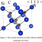 |
Figure 1: The crystal structure of cubic silicon carbide polytype (3C-SiC). |
![Figure 2: The polytype distribution in circumstellar 3C-SiC from the Murchison carbonaceous chondrite [10]. (a) TEM image with scale bar of 0.1 µm, (b) high-resolution transmission-electron-microscopy (HRTEM) image with scale bar of 1 nm, and (c) atomic model of the 3C-SiC zone axis superimposed on a simulated lattice image.](http://www.orientjchem.org/wp-content/uploads/2017/06/Vol33No3_Enha_Saei_fig2-150x150.jpg) |
Figure 2: The polytype distribution in circumstellar 3C-SiC from the Murchison carbonaceous chondrite [10]. (a) TEM image with scale bar of 0.1 µm, (b) high-resolution transmission-electron-microscopy (HRTEM) image with scale bar of 1 nm, and (c) atomic model of the 3C-SiC zone axis superimposed on a simulated lattice image. |
Structure, Model and its Validation
The cross-sectional views of the SES TFET with 3C-SiC substrate and dopant pocket layer and the conventional SES TFET are shown in Figure 3. Recently, the DG silicon-based TFET structure has been demonstrated experimentally [38]. On the one hand, the heavily doped pocket region can be achieved by a tilt angled implant before the gate stack formation [31]. On the other hand, we recently presented the process flow by high-energy and low-current boron implantation with another mask after the pocket formation to fabricate the SES TFET [35].
Two simulated structures have gate length of 30 nm, body thickness of 15 nm and gate oxide thickness of 2 nm. The channel, source and drain doping concentrations of the structures were 1015, 1020 and 1020 cm−3, respectively. For the SES TFET with the dopant pocket, a heavily doped pocket with doping concentration of 1019 cm−3 at the source channel interface is structured.
All the device simulations were done in Silvaco ATLAS software[39]. For superior accuracy, the BTBT model was included using a non-local path tunneling model in the simulations. Furthermore, the Shockley–Read–Hall and Auger recombinations; concentration dependent mobility, bandgap narrowing effect, field dependent mobility and trap–assisted tunneling (TAT) models were used to model the recombination and generation in the highly doped regions. Also, we recently presented the validation of our simulation non-local BTBT model by tuning of the effective electron and hole masses as done in our earlier works [13, 15, 23, 35, 40].
![Figure 3: Schematic structure of (a) the SES TFET with 3C-SiC substrate and dopant pocket and (b) the conventional SES TFET [38].](http://www.orientjchem.org/wp-content/uploads/2017/06/Vol33No3_Enha_Saei_fig3-150x150.jpg) |
Figure 3: Schematic structure of (a) the SES TFET with 3C-SiC substrate and dopant pocket and (b) the conventional SES TFET [38]. |
Results and Discussion
The effect of the 3C-SiC substrate and dopant pocket on the drain current of a SES TFET with 30 nm gate length versus the gate voltage (VGS) in linear and logarithm scales biased at the constant drain voltage (VD = 0.7 V) is shown in Figure 4. As seen, the extended source TFET with the 3C-SiC substrate and pocket exhibits higher on-current (more than 10 times) as compared to conventional extended source TFET due to the increase in the BTBT generation rate and reduced losses. This improvement in the BTBT generation rate is due to the existence of the n-type pocket at source and the channel interface. In the other words, the barrier width at the interface of source and channel is decreased for a TFET with the dopant pocket layer, which helps in the total electric field and drive current improvement, as mentioned in the Refs. 25, 31–34.
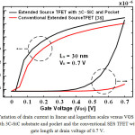 |
Figure 4: Variation of drain current in linear and logarithm scales versus VGS for the SES TFET with 3C-SiC substrate and pocket and the conventional SES TFET with 30 nm gate length at drain voltage of 0.7 V. |
Figure 5 illustrates the alteration of transconductance (gm) versus VGS for the extended source TFET with 3C-SiC substrate and pocket and conventional SES TFET with 30 nm gate length. It is evident that the extended source TFET with 3C-SiC substrate and pocket has higher transconductance values than the conventional extended source TFET because the improvement of drain current leads to an increase in the transconductance.
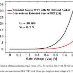 |
Figure 5: Variation of transconductance (gm) versus of VGS for the SES TFET with 3C-SiC substrate and pocket and conventional SES TFET with 30 nm gate length at drain voltage of 0.7 V. |
Figure 6 compares the switching-state current ratio for the extended source TFET with 3C-SiC substrate and pocket and conventional extended source TFET at drain voltage of 0.7 V. The current at off and on states are defined as the minimum value of drain current (as the current when VGS =0 V and VDS = 0.7 V) and the value of current when VGS = VDS = 0.7 V, respectively. As can be seen, the switching-state current ratio improves for he extended source TFET with 3C-SiC substrate and pocket. Its value is about 1013 for 100 nm extended source TFET with pocket.
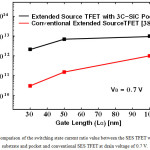 |
Figure 6: Comparison of the switching state current ratio value between the SES TFET with 3C-SiC substrate and pocket and conventional SES TFET at drain voltage of 0.7 V. |
Figures 7 and 8 show the gate voltage dependent gate to drain and gate to source capacitances of the SES TFET with 3C-SiC substrate and pocket and conventional SES TFET with 30 nm gate length at drain voltage of 0.7 V, respectively. The lower gate to source capacitance in the extended source TFET with 3C-SiC substrate and pocket is due to the barrier width reduction at the source to channel edge. However, due to the inversion layer extension from the drain-side toward the source-side, the dominant capacitance between the gate and the inversion layer under a TFET gate is gate-drain capacitance [25, 35].
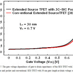 |
Figure 7: The gate voltage dependence of gate to drain capacitance of the SES TFET with 3C-SiC substrate and pocket and conventional SES TFET with 30 nm gate length at drain voltage of 0.7 V. |
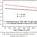 |
Figure 8: The gate voltage dependence of gate to source capacitance of the SES TFET with 3C-SiC substrate and pocket and conventional SES TFET with 30 nm gate length at drain voltage of 0.7 V. Click here to View figure |
Figure 9 illustrates the effect of the 3C-SiC substrate and dopant pocket on the channel resistance (Rch) of a SES TFET with 30 nm gate length versus the gate voltage biased at drain voltage of 0.7 V. It can be seen that the channel resistance value of the SES TFET with 3C-SiC substrate and pocket is much lower than that of the conventional SES TFET due to the high channel conductivity induced the existence of the n-type pocket at the interface of source and channel.
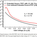 |
Figure 9: Channel resistance of the SES TFET with 3C-SiC substrate and pocket and conventional SES TFET with 30 nm gate length biased at drain voltage of 0.7 V versus VGS. Click here to View figure |
The channel resistance of the device plays a crucial role in determining transport time delay since Rch×Cgd acts as an index for showing of the channel charges response speed to gate signal [25, 35]. The variation in the transport time delay versus the gate voltage for the SES TFET with 3C-SiC substrate and pocket and conventional SES TFET with 30 nm gate length at drain voltage of 0.7 V is shown in Figure 10. As can be confirmed from Figure 9, due to the smaller resistance of channel, the transport time delay for the SES TFET with 3C-SiC substrate and pocket (about 0.15 psec) is much lower than that of conventional SES TFET.
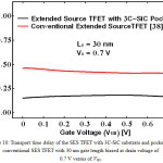 |
Figure 10: Transport time delay of the SES TFET with 3C-SiC substrate and pocket and conventional SES TFET with 30 nm gate length biased at drain voltage of 0.7 V versus of VGS. |
The cutoff and maximum oscillation frequencies are considered as figures of merit (FoM) for frequency response in the high frequency application. The RF performances of the SES TFET with 3C-SiC substrate and pocket are considered by extracting the cutoff and maximum oscillation frequencies and are compared with the conventional SES TFET. The cutoff and maximum oscillation frequencies are frequencies at which the current and unilateral power gains of a TFET drops to unity, respectively [25, 35]. Figure 11 displays the gate capacitance values of cutoff frequency for the SES TFET with 3C-SiC substrate and pocket and conventional SES TFET with 30 nm gate length as versus the gate voltage biased at drain voltage of 0.7 V. It is observed that the extended source TFET with 3C-SiC substrate and pocket shows better value of cutoff frequency when compared with that of the conventional SES TFET due to its higher transconductance, as shown in Figure 5.
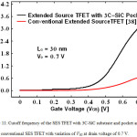 |
Figure 11: Cutoff frequency of the SES TFET with 3C-SiC substrate and pocket and conventional SES TFET with variation of VGS at drain voltage of 0.7 V.
|
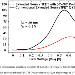 |
Figure 12: Maximum oscillation frequency of the SES TFET with 3C-SiC substrate and pocket and conventional SES TFET with variation of VGS at drain voltage of 0.7 V. |
Figure 12 shows the variation of maximum oscillation frequency of the SES TFET with 3C-SiC substrate and pocket and conventional SES TFET with 30 nm gate length versus the gate voltage at drain voltage of 0.7 V. It is evident that the extended source TFET with 3C-SiC substrate and pocket has higher maximum oscillation frequency than that of the conventional extended source TFET because it shows lower channel resistance and higher cutoff frequency, as seen in in Figures 9 and 11.
Conclusions
In this paper, we report a detailed study of the SES TFET with 3C-SiC substrate and dopant pocket layer. The variation in the DC and RF performances including the drain current, switching-state current ratio, gate to source capacitance, gate to drain capacitance, transconductance, channel resistance, transport time delay, cutoff frequency and maximum oscillation frequency as a function of gate voltage has been analyzed. The presence of the silicon carbide polytype as substrate and pocket in the channel at the source edge provides higher on-current about 10 times when compared with the conventional extended source TFET. A higher switching-state current ratio (∼1013), a smaller transport time delay (about 0.15 psec); and excellent cutoff and maximum oscillation frequencies were obtained, indicating that the SES TFET with 3C-SiC substrate and dopant pocket is a good candidate as a replacement for the conventional TFETs in future low power applications.
References
- Choyke, W. J.; Matsunami, H.; Pensl, G.; Silicon carbide: recent major advances, Springer, 2003.
- Cheung, R.; Silicon carbide microelectromechanical systems for harsh environments, Imperial College Press, 2006.
CrossRef - Marjani, S.; Faez, R.; Marjani, H.; Asian J. Chem. 2012, 24, 2333–2335.
- Marjani, S.; Faez, R.; Hosseini, S. E.; Asian J. Chem. 2013, 25, 4715–4717.
- Goel, S.; Journal of Physics D: Applied Physics, 2014, 47, 243001-1–243001-36.
- Bushchow,K. H. J.; Cahn, R. W.; Flemings, M. C.; Ilschner, B.; Kramer, E. J.; Mahajan, S.; and Veyssiere P.; Encyclopedia of materials: science and technology, Elsevier, 2001.
- Daulton, T. L.; Bernatowicz, T. J.; Lewis, R. S.; Messenger, S.; Stadermann, F. J.; Amari, S.; Science 2002, 296,1852–1855.
CrossRef - Vallett, A.; Minassian, S.; Kaszuba, P.; Datta, S.; Redwing J. M.; Mayer T. S.; Nano let. 2010, 10, 4813–4818.
CrossRef - Ionescu, A. M.; Riel, H.; Nature 2011, 479, 329–337.
CrossRef - Guo, P.; Yang, Y.; Cheng, Y.; Han, G.; Pan, J.; Ivana, Zhang, Z.; Hu, H.; Shen, Z. X.; Chia, C. K.; Yeo, Y.; J. Appl. Phys. 2013, 113, 094502-1–094502-9.
CrossRef - Zhu, Y.; Jain, N.; Mohata, D. K.; Datta, S.; Lubyshev, D.; Fastenau, J. M.; Liu, A. K.; Hudait, M. K.; J. Appl. Phys. 2013, 113, 024319-1–024319-5.
CrossRef - Datta, S.; Liu, H.; Narayanan, V.; Microelectronics Reliability. 2014, 54, 861–874.
CrossRef - Marjani, S.; Hosseini, S. E.; Faez, R.; AIP Advances 2016, 6, 095010-1–095010-7.
CrossRef - Li, M. O.; Esseni, D.; Nahas, J. J.; Jena, D.; Xing, H. G.; IEEE J. Electron Devices Soc. 2015, 3, 200–207.
CrossRef - Marjani, S.; Hosseini, S. E.; Faez, R.; J. Comput. Electron. 2016, 15, 820–830.
CrossRef - Wang, L.; Yu, E.; Taur, Y.; Asbeck, P.; IEEE Electron Device Lett. 2010, 31431–433.
- Trivedi, A. R.; Ahmed, K. Z.; Mukhopadhyay, S.; IEEE Electron Device Lett. 2015, 36, 201–203.
CrossRef - Luisier, M.; Klimeck, G.; J. Appl. Phys. 2010, 107, 084507-1–084507-6.
CrossRef - Britnell, L.; Gorbachev, R. V.; Jalil, R.; Belle, B. D.; Schedin, F.; Mishchenko, A.; Georgiou, T.; Katsnelson, M. I.; Eaves, L.; Morozov, S.
CrossRefV.; Peres, N. M. R.; Leist, J.; Geim, A. K.; Novoselov, K. S.; Ponomarenko, L. A.; Science 2012, 335, 947–950.
CrossRef - Ganapathi, K.; Yoon, Y.; Salahuddin, S.; Appl. Phys. Lett. 2010, 97, 033504-1–033504-3.
CrossRef - Lam, K-T.; Cao, X.; Guo, J.; IEEE Electron Device Lett. 2013, 34, 1331–1333.
CrossRef - Boucart, K.; Ionescu, A. M.; Solid State Electron 2007, 51, 1500–1507.
CrossRef - Baruah, R. K.; Paily, Roy P.; J. Comput. Electron 2015, 14, 492–499.
CrossRef - Narang R.; Saxena, M.; Gupta, R. S.; Gupta, M.; IEEE Trans. Nanotechnol. 2013, 12, 951–957.
CrossRef - Marjani, S.; Hosseini, S. E.; J. Appl. Phys. 2015, 118, 095708-1–095708-8.
CrossRef - Bal, P.; Ghosh, B.; Mondal, P.; Akram, M. W.; Tripathi, B. M. M.; J. Comput. Electron 2014, 13, 230–234.
CrossRef - Pandey, P.; Vishnoi, R.; Kumar, M. J.; J. Comput. Electron 2015, 14, 280–287.
CrossRef - Jain, P.; Prabhat, V.; Ghosh, B.; J. Comput. Electron 2015, 14, 537–542.
CrossRef - Lattanzio, L.; De Michielis, L.; Ionescu, A. M.; Solid State Electron. 2012,. 74, 85–90.
CrossRef - Revelant, A.; Villalon, A.; Wu, Y.; Zaslavsky, A.; Royer, C. L.; Iwai, H.; Cristoloveanu, S.; IEEE Trans. Electron Devices 2014, 61, 2674–2681.
CrossRef - Nagavarapu, V.; Jhaveri, R.; Woo, J. C. S.; IEEE Trans. Electron Devices 2008, 55, 1013–1019.
CrossRef - Cho, S.; Kang, I. M.; Current Appl. Phys. 2012, 12, 673–677.
CrossRef - Marjani, S.; Hosseini, S. E.; in Proc. the third conference on millimeter-wave and terahertz technologies (MMWATT), 2014, Tehran, Iran, 1–4.
- Abdi, D. B.; Kumar, M. J.; Superlattices and Microstructures 2015, 86,. 121–125.
CrossRef - Marjani, S.; Hosseini, S. E.; Superlattices and Microstructures 2014, 76, 297–314.
CrossRef - Marjani, S.; Hosseini, S. E.; in Proc. the 22st Iranian Conference on Electrical Engineering (ICEE), 2014, Tehran, Iran, 399–402.
- Marjani, S.; Hosseini, S. E.; in Proc. the 23st Iranian Conference on Electrical Engineering (ICEE), 2015, Tehran, Iran, 1042–1046.
- Krishnamohan, T.; Kim, D.; Raghunathan, S.; Saraswat, K.; in Proc. the IEEE international electron device meeting (IEDM), 2008, San Francisco, USA, 1-3.
- ATLAS Device Simulation Software, Silvaco Int., Santa Clara, CA, USA, 2012.
- Marjani, S.; Hosseini, S. E.; Journal of Electrical Systems and Signals, 2015, 3, 9–14.

This work is licensed under a Creative Commons Attribution 4.0 International License.


