TiO2 Thin Film’s Fabrication and Characterization in Response to Heat Treatment
Sunil Kumar* , Hansraj Sharma, Jagavendra Yadav
, Jagdish Prasad, and Mangej Singh
Department of Physics, University of Rajasthan, Jaipur, India.
Corresponding Author E-mail: sunilnehra161196@gmail.com
DOI : http://dx.doi.org/10.13005/ojc/400424
Article Received on : 26 Mar 2024
Article Accepted on : 20 Aug 2024
Article Published : 29 Aug 2024
Reviewed by: Dr. Hysen Thomas
Second Review by: Dr. Bena Ezhil
Final Approval by: Dr. B .K Sharma
In this study, substrates of glass were used for the deposition of transparent nanostructured thin layers of Titanium dioxide (TiO2) using a spin-coating system, and the solution was processed by sol-gel process. TiO2 sol and films were prepared with TTIP, hydrochloric acid, DI water, and ethanol. Here is the current work, these thin films were analyzed for various annealing treatments at 300 ◦C, 400 ◦C, 500 ◦C. The various attributes of films such as structural are described by X-ray diffraction (XRD) and RAMAN spectroscopy, morphology, and topography are studied by SEM and AFM, and optical properties are examined by UV-VIS spectroscopy. The direct energy bandgap estimated for the TiO2 films is 3.65ev, 3.71ev, and 3.75ev after heating at 300 ◦C- 400 ◦C- 500 ◦C. The initial crystalline phase (anatase) of TiO2 shows up after 400 ◦C for the four layers which are confirmed by XRD and RAMAN studies. At high temperatures, brookite and rutile crystalline phases are also found with the anatase phase. The attained films are translucent in the wavelength range between 380-700 nm and blurred in the 100- 380 nm range.
KEYWORDS:AFM; Raman Spectroscopy; Sol-gel; Spin coating; SEM
Download this article as:| Copy the following to cite this article: Kumar S, Sharma H, Yadav J, Prasad J, Singh M. TiO2 Thin Film’s Fabrication and Characterization in Response to Heat Treatment. Orient J Chem 2024;40(4). |
| Copy the following to cite this URL: Kumar S, Sharma H, Yadav J, Prasad J, Singh M. TiO2 Thin Film’s Fabrication and Characterization in Response to Heat Treatment. Orient J Chem 2024;40(4). Available from: https://bit.ly/3Z52F0G |
Introduction
Environmental improvement with TiO2 photocatalyst is receiving huge attention today because of the rise in environmental issues 1. TiO2 is a suitable material Because of many prime physical properties that are required for thin film applications. TiO2 also has prime chemical, optical, and electrical properties, making it useful in a variety of optical applications, including- gas-sensors 2, multiple-layer optical filters 3, photocatalytic water purification 4, planer waveguides 5. TiO2-based solar cells (especially- DSSCs) are a popular area of exploration due to their economical, easy manufacturing, environment friendly, and comparatively good energy conversion efficiency 6. TiO2 shows good transmittance, high bandgap, high dielectric constant, chemical stability, low cost, non-toxicity, and the capability to be readily doped with ions 7-9.
Because of its importance in applied physics, we can use various techniques in the TiO2 thin film preparation like chemical vapor deposition (CVD) [10], sputtering 11, and sol-gel method 12. The condition of synthesis and chemistry of the surface will affect the TiO2 thin film stability. Herein, the sol-gel procedure was adopted because it is simple and reproducible 13.
The Sol-gel procedure has several advantages in comparison to other approaches. The Sol-gel procedure shows excellent control of the chemistry, purity, homogeneity, and crystalline phase because of its simple use and economical machinery. The sol-gel method can retrieve new morphology and new physical properties 14.
The properties of TiO2 thin film can be modified by different heat temperature treatments. When we increase the temperature, the particle size of TiO2 increases, resulting in precipitate formation 15. Usually, the initial crystalline phase (anatase) of TiO2 is secure up to 400 °C, it transforms into the rutile phase at a higher temperature, which has less photoactivity for solar cells. This conversion takes place at about 500 °C temperature 16. By doping metallic ions in varying ratios, we can influence the phase conversion from anatase to rutile and the band-gap energy of TiO2. We can control band-gap energy and the anatase to the rutile phase transition of TiO2 by doping metallic ions in various ratios. The factors impacting the stability of the doped TiO2 are oxidation state, bonding of dopant, and ionic radius, it also improves the photocatalytic activity 17.
To enhance the qualities of solar applications, the current study aims to synthesize and characterize multiple TiO2 thin film properties, such as its makeup, morphology, and optics, at 3 different annealing temperatures: 300, 400, and 500 °C. We prepared TiO2 sol using the sol-gel method, and we applied TiO2 to plain substrates made of glass using the spin coating technique. The optical, morphological, and structural outcomes have been analyzed for the photovoltaic device’s stability, performance, and capacity.
Experimental
Cleaning process of the glass substrates
We cleaned simple glass substrates sequentially in ethanol, isopropanol, acetone, and then in Deionized water for 10 minutes each. Substrates were kept under Deionized water before use.
Chemicals
TTIP [Ti(O-i-C3H7)4], ethanol (CH3CH2OH), HCl (“Hydrochloric Acid”), and DI water all materials obtained from CDH Pvt. LTD, Daryaganj, Delhi. All the materials are AR grade for the preparation of TiO2 sol.
Solution Preparation Methodology
Firstly, we take 25 ml Ethanol (CH3CH2OH) and 0.1 Mol TTIP [Ti(O-i-C3H7)4] in a beaker Stirred for 2.30 hr at 50 0C. A solution of 25 ml Ethanol+0.1mol HCl+0.1 mol DI WATER was added by dropper and Stirred for 2.30 hr at 50 0C. then we received a Transparent TiO2 solution. After that, the prepared solution was spin-coated onto a non-conducting glass substrate at 2200 RPM for 40 sec. The deposited TiO2 thin films have been baked on a hot plate at 110ᵒC for 3 minutes to remove the solvents and other impurities. After that heat the baked film at 300ᵒC, 400℃, and 500 0C temperature for 30 min.
Characterization Methods
The X-rd machine (Panalytical X Pert Pro) was employed to the microstructures of the TiO2 nanocomposites at a temperature of 22℃. The crystal size is evaluated using Scherrer’s equation. The FESEM (Nova Nano FE-SEM 450) investigated the surface morphology and chemical configuration. Atomic force microscopy (AFM) having a Multimode Scanning Probe Microscope (Bruker) was employed to investigate the topographical feature.
The absorbance and transmittance measurements of films were analyzed as a sample and non-conducting glass as a standard using UV Spectrophotometer-LAMBDA-750-UV-Vis-NIR. Raman spectroscopy (STR 500 CONFOCAL MICRO) was employed to determine the Raman shift.
Chemical Composition
Spin-coated TiO2 thin films have undergone an energy dispersive spectroscopy (EDS) analysis to ascertain the presence and reveal the chemical makeup of components. The EDS spectrum shows four principal peaks, three for Ti and one for O. The existence of Ti and O materials, as well as their atomic percentages, were verified by EDS analysis. According to EDS analysis, the highlighted atomic concentration in thin films of TiO2 matches the predicted proportion of atoms at 500°C annealing temperature. The EDS plot is revealed below in Figure (1). Table 1 comprises TiO2 thin film EDS data.
 |
Figure 1: Chemical composition of TiO2 thin film annealed at 500℃ |
Table 1: Composition of TiO2 in Atomic % of composition
|
Elements |
Atomic % |
Weight % |
|
Ti |
38.57 |
64.67 |
|
O |
62.78 |
36.06 |
Structural Study
X-Rd patterns have been applied to examine the crystalline phase and size of the crystallite of the deposited nanostructured thin film of TiO2 at various annealing temperatures of 300, 400, and 500 0C. At the post-annealing temperature of 300 ℃, we did not get any peak, and it shows an amorphous graph. After that, when the annealing temperature goes to 400 0C, the X-rd pattern shows a single peak at 2Ѳ =250.3635’. It is identified as the anatase phase at the peak (1 0 1).
The anatase phase of the peak (101) becomes sharper with the increase in the heat treatment. that shows that crystal size is increasing concerning increasing in annealing temperature. The anatase phase starts to transform into the rutile and brookite phase gradually when we increase the annealing temperature 18.
At 500 0C annealing temperature, X-rd spectra show three peaks at 2Ѳ of 25.26920, 37.79280, and 48.00080, which correspond to the lattice planes (1 0 1), (0 0 4), and (2 0 0). The blend of both anatase and rutile phase structure in the final TiO2 film has been analyzed. In this mixture, the anatase phase has more influence because of the high activity of photocatalysis 19.
The crystalline size has been increased with the increase in heat treatment as can be seen in table (2).
Table 2
|
Annealing temp. |
Crystallite Size(nm) |
|
400 0C |
2.10 |
|
500 0C |
3.16 |
Here we evaluate crystal size(D) by Scherrer’s equation-
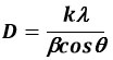
D indicates the average of the crystalline, k represents the shape factor, λ signifies the Cu-Kα x denotes ray wavelength, β indicates the FWHM (“Full Width Half Maxima”), θ presents the Bragg-angle.
The average crystallite size of TiO2 thin film made using the sol-gel methodology and accumulated by spin coating process at 2000 rpm for 30 sec came out to be 2.10 nm at 400 0C and 3.1601 nm at 500 0C.
Dislocation density (ẟ)- Williamson and Smallman’s formula (e) was utilized to determine the ẟ present in the TiO2 thin film.

The determined ẟ value for TiO2 thin film is 0.2267 nm-2 and 0.07672 nm-2.
The Raman spectra display distinct peaks linked to the attendance of TiO2 in anatase and brookite phases at annealing temperatures of 4000C and 5000C. Bands about 153 and 193 cm-1 are ascribed to the TiO2 anatase phase in these spectra 20.
 |
Figure 2: XRD pattern of TiO2 films annealed at various temperatures |
|
|
Figure 3: Raman spectra of TiO2 thin film at different temperature |

Investigation of optical characteristics
The optical features of thin films of TiO2 can be analyzed with Transmittance spectra (Fig), absorbance spectra (fig-5), and reflectance spectra (fig-6) from 200 to 800 nm which are displayed. The transparency on average is 80% in the visible range. The film transmission aggrandized moderately in the influence of annealing temperature in the near-infrared region. An incisive decrease is observed in each absorbance spectra at 300–345 nm probably because of imperfection in the crystallinity of the material. The Tauc expression is applied to compute the energy band gap (Eg) 21:
Where α, h, Eg, A, and n have their usual meaning
A straight line with an intercept to the X-axis is expected to offer the optical band gap in its direct form on a graph between (αhν)2 and hν. The curve between (αhν)2 and hν is displayed in fig. (6). The essence of acquired data shows that TiO2 thin films have a direct band-gap- gap and when the annealing temperature was increased the direct band-gap was decreased. This acquired band gap was higher than the proclaimed optical band gap for single-crystal 3.2 ev. The large optical band gap value obtained for spin-coated TiO2 thin film might be because of the quantum size impact and size of finite crystallite 22.
 |
Figure 4: UV transmittance spectrum of the TiO2 |
 |
Figure 5: UV absorption spectrum of the TiO2 |
 |
Figure 6: Band – Gap Graph of the TiO2 |
Surface morphology study
SEM was employed to investigate the shape of the surface (surface morphology) and the dispersion of pores of the developed films. Its images show particles are divergent, spherical, and extended, with large particle size distribution. SEM investigates morphological changes of annealed TiO2 thin films from 300 0C, 400 0C, and 500 0C confirming that the surface morphology of the film has been modified with the annealing temperature.
Fig. (7) displays the SEM images in the top view, and it is examined that the larger particles are made of smaller fragments, the distance between nanoparticles reduces with the rising temperature, and thin films will be more closely packed. The SEM analysis verifies that annealing temperature treatment plays a vital role in the morphology of TiO2 thin film, thus the crystallization of layers. Above, X-rd data and AFM also support the SEM observations that the size of crystallite increases from 300 0C to 500 0C as a result of densification.23.
 |
Figure 7: SEM micrographs of the TiO2 at post-heat treatment (a.) 300 ℃ (𝑏) 400 ℃ & (c.) 500 ℃ |
AFM is utilized to check the surface morphology mitigation and evaluation of TiO2 thin films at 500 0C annealing temperature. AFM images at 500 0C (Fig. 8) show that the grain agglomeration is in a satisfactory state.
 |
Figure 8: AFM images of the TiO2 thin film annealed at 500 ℃ |
Conclusion
This study describes the formation and characteristics of the TiO2 thin films employing a simple and economical method: sol-gel spin coating methodology. As it generates samples with high homogeneity and repeatability, the sol-gel method is acknowledged as one of the most straightforward procedures for preparing TiO2 thin films and the most effective in terms of layer quality. The deposition was carried out at a temperature of 22 ℃ and post-annealed at distinct temperatures of 300 ℃-400 ℃-500 ℃. The influence of temperature on the features of TiO2 is discussed in this study.
The X-rd pattern reveals an amorphous graph at an annealing temperature of 300 ℃, it shows an anatase phase around 400 ℃. Furthermore, at a higher annealing temperature (500 ℃), it shows the presence of both initial phases (rutile-anatase) of TiO2. The Raman spectra also help this fact.
The SEM microscopy shows no breaks in the film, which is made up of microscopic flaky clusters at 300 ℃ heat treatment. Further, grain size increases with an increase in heat treatment. The study of UV-Vis spectra reveals that absorbance decreases abruptly around wavelength 340-345 nm and the band gap increases gradually with increasing temperature.
Acknowledgment
We are thankful to MNIT Jaipur and Manipal University, Jaipur for providing facilities for this work and also grateful to USIC, Rajasthan University, Jaipur.
Conflict of Interest
There is no disagreement of interest, as stated by the corresponding author with the permission of all authors.
Funding Sources
The author(s) received no financial support for the research, authorship, and/or publication of this article.
Data availability
Yes, Original data is available
Ethical approval
The experiment and study do not involve the use of humans or animals.
References
- Jiaguo Yu, Xiujian Zhao, Qingnan Zhao, Photocatalytic activity of nanometer TiO2 thin films prepared by the sol-gel method, Materials Chemistry and Physics 69(2001) 25-29.
CrossRef - Tian Xu, Xiuxiu Cui, Tingrun Lai, Ren Jie, Zhichao Yang, Mingjing Xiao, Bingsen Wang, Xuechun Xi ao, Gas sensors based on TiO2 nanostructured materials for the detection of hazardous gases: A review, Nanomaterial science, Volume 3, Issue 4, December 2021, Pages 390-403
CrossRef - Asghar M. H., Shoaib M., Placido F., Naseem S., Wide bandpass optical filters with TiO2 and Ta2O5, Cent. Eur. J. Phys. • 6(4) • 2008 • 853-863
CrossRef - Riaz S., Park S.J., An overview of TiO2-based photocatalytic membrane reactors for water and wastewater treatments, Journal of Industrial and Engineering Chemistry 84 (2020) 23–41.
CrossRef - Lukowiak A., Dylewicz R. , Patela S. , Stre W. , Krzysztof Maruszewski . Optical properties of SiO2–TiO2 thin film waveguides obtained by the sol–gel method and their applications for sensing purposes, Optical Materials 27 (2005) 1501–1505.
CrossRef - Baraton M.I., Nano-TiO2 for Dye-Sensitized Solar Cells, Recent Patents on Nanotechnology 2012, 6, 10-15.
CrossRef - Mechiakh R., Meriche F., Kremer R., Bensaha R., Boudine B., Boudrioua A., TiO2 thin films prepared by sol–gel method for waveguiding applications: Correlation between the structural and optical properties, Optical Materials 30 (2007) 645-651.
CrossRef - Kumar S., Sharma H., Parsad J., Yadav J, Effect of Ag ion Implantation on the Crystallinity and Optical Property of Spin-coated TiO2 Thin Films, Oriental Journal of Chemistry, Volume 39, Number 4 (2023)
CrossRef - Zhao Z, Sun J, Xing S, Liu D, Zhang G, Bai L, and Jiang B (2016) J. Alloys Compd. 679 88.
CrossRef - Yeung K. S. and Lam y. W., a simple chemical vapor deposition method for depositing thin tio2 films, thin solid films, 109(1983), il69-178.
CrossRef - Shao C., Wang W. H., Hsu M. Y., Wang L. C., Characteristics of ion-beam-sputtered high-refractive- index TiO2-SiO2 mixed films”, J. Opt. Soc. Am. A 16(1999), P1477.
CrossRef - Halin D. S. C., Abdullah M. M. A. B., Mahmed N., Abdul Malek S. N. A., Vizureanu P. and Azhari A. W., Synthesis, and Characterization of TiO2/SiO2 Thin Film via SolGel Method, Materials Science and Engineering 209 (2017) 012002.
CrossRef - Akpan U.G., Hameed B.H., the advancements in sol–gel method of doped-TiO2 photocatalysts, Applied Catalysis A: General 375 (2010) 1–11.
CrossRef - Naseri N., Amiri M. and Moshfegh A. Z., Visible photo enhanced current-voltage characteristics of Au: TiO2 nanocomposite thin films as photoanodes, J. Phys. D: Appl. Phys. 43 (2010) 105405 (8pp).
CrossRef - Timoumi A., Albetran H.M., Alamri H.R., Alamri S.N., Low I.M., Impact of annealing temperature on structural, morphological and optical properties of GO-TiO2 thin films prepared by spin coating technique, Superlattices and Microstructures 139 (2020) 106423.
CrossRef - Lin C.P., Chen H., Nakaruk A., Koshy P., Sorrell C.C., Effect of Annealing Temperature on the Photocatalytic Activity of TiO2 Thin Films, Energy Procedia 34 (2013) 627 – 636.
CrossRef - Kumaravel V., Rhatigan SMathew S., Bartlett J., Nolan M., Hinder S.J., Sharma P.K., Singh A., Byrne J.A., Harrison J., Pillai S.C., Indium -Doped TiO2 Journal Pre-proof Journal Pre-proof Photocatalysts with High -Temperature Anatase Stability, J. Phys. Chem. C. 123 (2019) 21083 –21096.
CrossRef - Zhoua B., Jianga X., liub Z., Shena R., Rogachev A.V., Preparation and characterization of TiO2 thin film by thermal oxidation of sputtered Ti film, Materials Science in Semiconductor Processing 16 (2013) 513–519.
CrossRef - Rao1 M.C., Ravindranadh K. and Shekhawat M.S., Structural and Electrical Properties of TiO2 Thin films, International Conference on Condensed Matter and Applied Physics (ICC 2015) AIP Conf. Proc. 1728, 020077-1–020077-4.
- Ibrahim A. Alhomoudi, Newaz, Residual stresses and Raman shift relation in anatase TiO2 thin film, Thin Solid Films 517 (2009) 4372–4378.
CrossRef - Senthil T.S., Muthukumarasamy N., Agilanb S., Thambidurai M., Balasundaraprabhuc R., Preparation and characterization of nanocrystalline TiO2 thin films, Materials Science and Engineering B 174 (2010) 102–104.
CrossRef - Fouzia A., Rabah B., The influence of doping lead and annealing temperature on growth of nanostructures of TiO2 thin films prepared by a sol-gel method, Materials Science and Engineering, Volume 265, March 2021, 114982.
CrossRef - Jagavendra, Jagdish Prasad, Hansraj Sharma, Sunil Kumar, and Mangej Singh. “Effect of Zn and Sn incorporation on the crystallinity of spin-coated CuInSe2 thin films.” Journal of Materials Science: Materials in Electronics 33, no. 24 (2022): 19119-19128.
CrossRef

This work is licensed under a Creative Commons Attribution 4.0 International License.
About The Author
![]()
A New Edition of Web of Science
Journal Impact Factor
2022: 0.5
Five Year: 0.8
Journal is Indexed in

Cabells Whitelist
![]()


