Effect of nanograin sublayers on structure and properties of the electrodeposited ZnO arrays
V. V. Ivanov1, G. V. Tsepilov1, I. V. Iyenyutin2 and A. N. Voropay1
1Technocomplekt closed joint stock company, Shkol’naya str., 10a, Dubna, Moscow area (oblast), 141981 Russia.
2Turboenergoremont,Leninskiy prospect 114, block. А, premises 170Н, Saint Petersburg, Leningradskaya area (oblast), 198207, Russia.
Corresponding author Email: mtrushin@mail.ru
DOI : http://dx.doi.org/10.13005/ojc/320233
Article Received on :
Article Accepted on :
Article Published : 07 May 2016
The influence of ZnO nanograin sublayers deposited at the initial stage of the electrodeposition on morphology, structure, optical and electrical properties of the nanostructured arrays of this material produced in the pulsed electrodeposition mode has been investigated. It is shown that the formation of these sublayers contributes to enlargement of the crystal grains and the formation of separate zinc oxide nanorods, which are perpendicular to the surface of the substrate. Moreover, the zinc oxide array electrodeposited in the pulsed mode with using nanograin sublayers has higher specific resistance, better transparency, scatters less visible light and has an appropriate optical band gap.
KEYWORDS:pulsed electrodeposition; 1-D ZnO; structure; optical properties; AFM
Download this article as:| Copy the following to cite this article: Ivanov V. V, Tsepilov G. V, Iyenyutin I. V, Voropay A. N. Effect of nanograin sublayers on structure and properties of the electrodeposited ZnO arrays. Orient J Chem 2016;32(2) |
| Copy the following to cite this URL: Ivanov V. V, Tsepilov G. V, Iyenyutin I. V, Voropay A. N. Effect of nanograin sublayers on structure and properties of the electrodeposited ZnO arrays. Orient J Chem 2016;32(2). Available from: http://www.orientjchem.org/?p=15886 |
Introduction
Zinc oxide (ZnO) belongs to the rapidly developing class of materials used for electronic and optoelectronic applications 1-9. The reason is not only in the unique properties of this wide bandgap semiconductor (Eg = 3.37 eV) with direct optical transitions and a large exciton binding energy (60 MeV at the room temperature), but also in the possibility of obtaining ZnO using different technologies, including inexpensive and suitable for large-scale production of liquid-phase chemical and electrochemical methods 2-10. The another advantage of the material ZnO is its propensity to form nanostructures with different morphology among which the greatest interest for the developers of electronic products and optoelectronics attract nanowires and nanorods, i.e., one-dimensional (1-D) nanostructures of zinc oxide. The method of electrochemical deposition from aqueous solutions allows producing arrays of 1-D ZnO within 10 – 90 minutes on the large areas and at a temperature not exceeding 100 ° C 2-10. The efficiency of this method depends also by using readily available dilute solutions of zinc salts and sodium (or potassium) as starting materials. They typically do not contain modifying additives of complexing agents or surface-active organic substances that pollute the environment. The success of the method of electrodeposition is in the fabrication of optoelectronic devices, gas nanosensors, UV detectors, solar cells organic and hybrid photovoltaic cells is due to the fact that its use for the creation of nanostructures of zinc oxide combines such advantages as the simplicity of the technological equipment and the suitability for mass production with a good control of the process. In order to make a necessary morphology for the ZnO nanostructures, scientists 2-10 widely investigate the influence of cathode potential, the electrolyte composition, the temperature and the time of deposition, the presence or absence in the solution of various organic additives and complexes, the following hydrothermal treatments, the annealing and even the gravity on the structure and properties of electrodeposited arrays of zinc oxide. The electrolysis process is carried out in potentiostatic or galvanostatic conditions, i.e. at the constant potentials of the cathode or cathode current, respectively 2-4,8. However, as was shown in 5-7,9-10, the pulsed electrolysis provides a controlled growth of semiconductor nanostructures without the threat of contamination of organic or other impurities from the electrolyte. In 5-7,9-10 was demonstrated the possibility of controlling the morphology of the electrodeposited in pulsed arrays of zinc oxide in the same galvanic bath by varying the modes of cathodic pulsed electrochemical deposition of ZnO without rotation of the substrates and changes in the composition of the electrolyte.
Since the formation of 1-D ZnO in the electrodeposition is carried out by means of self-organization (the bottom-up analysis), the most important is the initial phase of the process, when on the surface of the foreign substrate the first crystal nuclei are formed. Therefore a sufficient attention was given for the creation of nanostring sublayers that are orienting the further growth of nanorods and nanowires of ZnO, although all the works 2-4,8 dealt with the electrolysis at constant currents or potentials. In this work for the first time examines the impact of nanograin sublayers of ZnO that are created at the initial stage of electrodeposition for the morphology, structure, optical and electrical properties of nanostructured arrays of zinc oxide, which are produced in the pulsed electrodeposition.
The methodology of the experiment
The fabrication of arrays of nanorods of zinc oxide was performed by the pulsed cathodic electrochemical deposition in a thermostated three-electrode electrochemical cell with the non-mixed aqueous electrolyte containing of 0.01 M Zn(NO3)2 and 0.1 M NaNO3 at a temperature of 70oC. As substrates (cathode, or working electrode) were used plate brand FTO TEC 7 Pilkington company, USA. A platinum spiral served as a counter-electrode and as the reference electrode – a saturated silver chloride electrode Ag/AgCl. In the manufacture of the ZnOsр sample (sp – seed and pulse), at the first stage of electrodeposition was created a nanograin ZnO sublayer by feeding in the same electrolyte at the FTO working electrode a constant potential of U = -1.3 V during 30 seconds. Then, using the impulse potentiostate PI-50-1.1, equipped with a programmer PR-8, for the implementation of pulse electrolysis for 10 minutes at a substrate-cathode were applied square waves of potential: the lower limit Uoff cathode potential was -0.7. In, the upper limit Uon = -1.3 V (the potentials are given relative to the reference electrode Ag/AgCl). The duty cycle, i.e. the ratio of pulse duration to the sum of impulse duration and pauses, and the frequency as the reciprocal of the sum of the durations of the pulse and the pause, were 0.4 and 2 Hz, respectively. A sample of zinc oxide by ZnOр (p – a pulse) was electrodepositioned in a same pulsed mode, and ZnOsр, but at the initial stage of its manufacture we did not create the nuclei sublayers using of potentiostatic electrolysis.
The study of the optical properties of nanostructured layers of zinc oxide was performed by a spectrophotometer SF-2000, which is equipped with a console of a mirror and diffuse reflection SFD-2000. As control samples during the registration of the spectrum of optical transmission T(λ) was used the FTO substrate. The optical width of the forbidden zone Еg of ZnO layers was determined similarly to that described in 10 by the extrapolation to the energy axis of the linear section of the dependence of
[-ln(T)·hν]2 against hν. The disordered structure of ZnO was evaluated by the value of Urbach energy Ео, which is determined by the angle of inclination of the linear section of the dependence of ln[-ln(T)] against hν. The light scattering factor (Hf, Haze factor) was calculated according to [10] as the ratio of diffuse reflectance to the total reflection R (the sum of diffuse and specular reflections).
To analyze the structural and substructural parameters of arrays of ZnO the X-ray spectra (XRD) were recorded using diffractometer DRON-4 in the radiation CoКα (λCoKα = 1.7889 Å). Scanning was carried out with focusing according to Bragg-Brentano (θ–2θ). Processing of the obtained X-ray diffraction patterns (background separation, the separation of the doublet Kα1 – Kα2 etc.), as well as the calculation of profile of diffraction lines were performed using programs “New_Profile v.3.4 (486)” and “OriginPro v.7.5”. The presence of crystalline phases was detected by comparing data of the experimental X-ray diffraction patterns with the JCPDS database of reference data using the program “PCPDFWIN v.1.30”. Evaluation of the regions of coherent scattering (RCS) and microstresses Δd/d (where d is the period of the crystalline lattice according to JCPDS, Δd is the difference between experimental and reference values of the period lattice) in arrays of zinc oxide was carried out by analyzing the broadening of X-ray diffraction peaks, with taking into the consideration the presence of the instrumental broadening by the method of approximations of Williamson Hall according to 11-12. The residual stress in ZnO was determined according to the methodology that was proposed in 11. To study the texture of electrodeposited arrays of zinc oxide by the method of Harris we used the values of integral intensities of X-ray diffraction peaks, in accordance with 13. For each peak, we calculated the value of the pole density P(hkl), which characterizes the probability with which the normal to the surface of the crystallite coincides with the normal to the plane (hkl), in another word, it determines the number of crystallites, and their plane (hkl) is parallel to the sample surface. A pole density was calculated for all reported X-ray diffraction peaks, the values of P(hkl) >1 was attributed to the axes of the texture.
The study of surface morphology of arrays of zinc oxide produced by the method of semi-contact atomic force microscopy (AFM) on the device “Nanolaboratory NTEGRA prima, NT-MDT”.
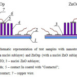 |
Figure 1: A schematic representation of test samples with nanostructured arrays of ZnOр (without a nuclei sublayer) and ZnOsp (with a nuclei ZnO sublayer) Click here to View figure |
To determine the type of conductivity of ZnO has been used the standard method of using a thermal probe [14]. To study the electrical properties of electrodeposited arrays of zinc oxide as vertically arranged on the FTO substrates ZnO nanorods, were fabricated metal contacts with Indium (In). Indium was chosen as the contact material because of its ratio of work output In (ΦIn = 4.09 eV) and the electron affinity to ZnO (χZnO = 4.2 eV), and it must ensure the formation of ohmic contacts with ZnO, according to 1,15, In order to avoid shunting, In vacuum deposition was performed under an angle of 70° to the surfaces of ZnO and FTO in their limited areas (0.1 x 1.0 cm) using a removable shadow mask made of aluminum. Then, on the surface of Indium was applied a conductive adhesive with a silver filler “Contactol” to attach to In copper microwires. The test samples which were manufactured in this manner and presented in figure 1 were used for measuring dark current-voltage characteristics (CVC) on the diagram of a curve tracer 16 by connecting to a commercial curve tracer L2-56 for a direct visualization of the CVC on the screen.
According to the results of CVC, measured in the case of the location of two Indium contacts on the surface of FTO, was obtained the total resistance Rt = U/I and was calculated resistivity ρFTO of FTO transparent conductive layer according to the formula:
pFTO = Rt: SFTO/w (1)
where SFTO – multiplication of the length of the Indium contact to the FTO layer thickness; w is the distance between two Indium contacts disposed on FTO.
By using the CVC we obtained a value of ρFTO = 3.5∙10-4 Ω∙cm, which corresponds to the data of the certificate for FTO of a brand of TEC 7 Pilkington company, USA. Calculations of the resistivity of the nanorods of zinc oxide ρZnO were based on measurements of CVC for Indium contacts between the top ends of the nanorods of zinc oxide, and FTO:
U/I = RΣ = pFTO. L/SFTO+ 2.pZno.t/Sc (2)
where RΣ is the total resistance derived according to CVC between two Indium contacts, one of them was located on FTO and the other was deposited on the upper ends of the nanorods of zinc oxide; L – the distance between these contacts; t ‒ the average length of the ZnO nanorod (t ≈ 0.4 μm); Sc – the Indium contact area; the coefficient 2 takes into account the total area of cavities between the ZnO nanorods.
If both contacts were located on the upper ends of the nanorods of zinc oxide, the obtained from the corresponding CVC the ratio U/I correspond to the expression:
U/I = RΣ = pFTO.∫/SFTO + 4pZnO. t/Sc (3)
where l – is the gap between the centers of the Indium contacts.
The study of the temperature dependence of the electrical conductivity of electrodeposited in a pulsed mode of ZnO nanostructured layers for measurement of their activation energy Ea was performed by analogy with the described in [17] by using a measuring stand, providing a temperature control of test samples in air atmosphere and measuring the change in the resistance of ZnO by decreasing the thermostat temperature and of the investigated sample in the range from 150 to 20° C. Depending on lgI from 1/T (where I is the current (A) flowing through the ZnO nanorods at a fixed voltage of 1.0 V; T is the temperature (K)) we determined the activation energy using the formula:
tg α= -0.43.Eα/k (4)
where Ea – an activation energy, j; k – Boltzmann constant, j/K.
Results and discussion
Figure 2 shows the X-ray diffraction pattern produced in the pulse regimen of the electrodeposition of nanostructured arrays of zinc oxide, obtained without the use of nuclei sublayer (ZnOр) and with using of nuclei sublayer (ZnOsр).
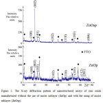 |
Figure 2: The X-ray diffraction pattern of nanostructured arrays of zinc oxide manufactured without the use of nuclei sublayer (ZnOр) and with the using of nuclei sublayer (ZnOsр). Click here to View figure |
Their analysis indicates that both arrays of ZnO are single-phase and have a hexagonal structure of the wurtzite modification (ZnO, JCPDS PDF#361451). The electrodeposited arrays of zinc oxide are nanocrystalline, and the area of coherent dispersion of ZnOр sample are in the range of 60 to 115 nm, and in the case of use in the electrodeposition of nuclei sublayers of area of coherent dispersion increase and range from 80 to 200 nm, which indicates to an improvement of the structure. Both samples characterized by low microstresses Δd/d ≈ 10-3, the compressive residual stress of 0.1 GPA is for ZnOр and 0.4 GPA for ZnOsр.
According to the calculations, unlike ZnOр, ZnOsр sample is characterized by larger crystal lattice parameters along the c axis (c = 5.22 Å) compared to the reference ZnO (according to JCPDS PDF#361451, C = 5.207 Å). On the other hand, the array of ZnOр is weakly textured in the direction <001>, i.e. in a perpendicular direction to the substrate surface (P(002) = 1.6), while the sample ZnOsр, fabricated with electrodeposition of the nuclei sublayer at the initial stage of growth, has a significant preferential orientation perpendicular to the substrate, as it has an axial texture of (002) = 3.2. Optical properties of electrodeposited nanostructured arrays of ZnO in a pulsed mode (figure 3) show a sufficiently high transparency and an evident absence of an interference pattern of 1-D ZnO in the optical transmission spectrum T(λ) (figure 3A).
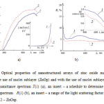 |
Figure 3: Optical properties of nanostructured arrays of zinc oxide manufactured without the use of nuclei sublayer (ZnOр) and with the use of nuclei sublayer (ZnOsр): optical transmittance spectrum Т(λ) (a), an insert – a schedule to determine Eg; optical reflection spectrum R(λ) (b), an insert – a range of the light scattering factor of Hf(λ) 1 – ZnOр; 2 – ZnOsр. Click here to View figure |
The width of the forbidden zone for direct optical transitions in ZnOр is 3.22 eV. For ZnOsр Eg = 3.37 eV (insert in figure 3, a), i.e., do not different from Eg for a single crystal ZnO. Accordingly, the value of Urbach energy, which is a measure of disorder patterns, is almost twice in ZnOр ( Ео = 0.45 eV) than in ZnOsр ( Ео = 0.29 eV). As you can see in the АFМ images of the surface of ZnOр and ZnOsр (figure 4) the diameters of the nanorods of the two samples are in the range from 300 to 500 nm. This explains large values of the factor of light scattering on the spectrums of Hf(λ), mainly due to diffuse reflection from arrays of ZnO, especially for ZnOр the range of wavelengths that are commensurable with the diameters of the nanorods (insert in figure 3, b).
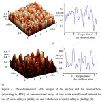 |
Figure 4: Three-dimensional АFМ images of the surface and the cross-sections (according to АFМ) of nanostructured arrays of zinc oxide manufactured without the use of nuclei sublayer (ZnOр) (a) and with the use of nuclei sublayer (ZnOsр) (b). Click here to View figure |
As follows from comparison of three-dimensional images of ZnOр and ZnOsр and the corresponding profiles of the cross section of these arrays (figure 4), using the stages of potentiostatic formation of the nanograin sublayer before the pulsed electrodeposition of zinc oxide contributes to the growth of free-standing nanorods of this material, while without such a sublayer of ZnO the nanorods are packed very tightly and, as a rule, are spliced.
A measurement method of using a thermal probe showed that both samples of zinc oxide which were electrodeposited in pulsed mode have a typical conductivity for ZnO n-type. According to [1,18–19], the n -type of ZnO conductivity may be due to the presence in its own crystal structure of native defects, in the first place, the non-structure defects of Znо, oxygen vacancies Vo and the interstitial Zni. In addition, as indicated in [18], the п -type films of zinc oxide may be caused by their unintentional doping by the interstitial hydrogen Hi, which acts as a shallow donor with an activation energy of about 30 MeV. In [19] is described that the energy level of the defect of Hi in ZnO is 0.03 – 0.05 eV.
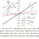 |
Figure 5: The dark CVC of nanostructured arrays of zinc oxide, which were electrodeposited without the use of nuclei sublayer (ZnOр) and with the use of the nuclei sublayer (ZnOsр). Upper insert ‒ dark CVC of FTO. The bottom inset is the temperature dependence of the electrical conductivity of the respective samples of zinc oxide. Click here to View figure |
1 – ZnOр; 2 – ZnOsр;3 – FTO.
As it was shown in [10], a cathodic reaction of a water recovery with hydrogen release at the potentials that are rather more negative than -1.05 V (Rel. Ag/AgCl) leads to the process of electrodeposition of ZnO, allowing more likely the intrusion of hydrogen into the crystal lattice of zinc oxide, especially at the stage of forming the nucleation layer at a constant potential of -1.3 V (Rel. Ag/AgCl). Figure 5 shows the ohmic nature of the dark CVC for both samples.
Calculations of the resistivity of ZnO gave the higher values of ρZnO for ZnOsр compared to ZnOр, 1·105 and 3·104 Ω·cm, respectively, that is possibly associated with a reduced conductivity of nanograion sublayer, that contributed to the average length of nanorod value ρZnO. The another probable reason of differences in a specific resistance of the samples ZnOsр and ZnOр can be [1,15,18] the anisotropy of electrical properties of polar planes, which include the (002) and nonpolar planes of the hexagonal lattice of the wurtzite. As noted above, our structural studies showed that ZnOsр has a much better texture (002) compared with ZnOр, and, consequently, a relatively larger number of polar planes at its surface. The third likely reason of the differences in conductivity of the samples ZnOsр and ZnOр is the width of the surface depletion region in ZnO, which is caused by adsorption of oxygen from the atmosphere and depends upon the texture of this material, and, in addition, depends on the surface morphology of nanostructured ZnO arrays [4,15]. The bottom inset in the figure 5 shows the activation energy Еа, that was defined using a dependency of lgI from 1/T, and it amounted of Еа = 0.04 eV for ZnOр and Еа = 0.06 eV for ZnOsр. According to [1,15,18-19], such activation energy indicates the presence in both samples of fully ionized at a room temperature shallow donor levels of Zni andHi.
Conclusion
In this work, we demonstrated the influence of ZnO nanograin sublayers which are created at the initial stage of electrodeposition, on the morphology, structure, optical and electrical properties of nanostructured arrays of 1-D ZnO, produced by the pulsed electrodeposition. It was shown that the formation of such sublayers contributes to the coarsening of crystal grains in the 1-D ZnO and the formation of separate zinc oxide nanorods, arranged perpendicularly to the surface of the FTO substrate. In addition, the electrodeposited array of zinc oxide in a pulsed mode using nanograin sublayers has a higher resistivity, better transparency, less scatters visible light and has a characteristic optical width of the forbidden zone for this material.
Acknowledgement
This article was prepared as a part of the implementation of applied research and experimental development (ARED) on the Agreement on the subvention (2015, October, 27) No. 14.579.21.0113 with the financial support of the Ministry of education and science of the Russian Federation. A unique identifier of ARED – RFMEFI57915X0113.
References
- Litton, C.W.; Reynolds, D.C.; Collins, T.C. Zinc oxide materials for electronic and optoelectronic device applications ., United Kingdom: John Wiley & Sons, Ltd., 2011.
CrossRef - Inamdar, A.I.; Mujawar, S.H.; Sadale, S.B.; Sonavane, A.C.; Shelar, M.B.; Shinde, P.S; Patil, P.S. Electrodeposited zinc oxide thin films: Nucleation and growth mechanism ., Solar Energy Materials & Solar Cells. 2007, 91, 864-870.
CrossRef - Tolosa, M.D.R.; Orozco-Messana, J.; Lima, A.N.C.; Camaratta, R.; Pascual, M.; Hernandez-Fenollosa, M.A. Еlectrochemical deposition mechanism for ZnO nanorods: diffusion coefficient and growth models ., Journal of The Electrochemical Society. 2011, 158, E107-E110.
- Skompska, M.; Zarębska, K. Electrodeposition of ZnO nanorod arrays on transparent conducting substrates–a review., Electrochimica Acta. 2014, 127, 467-488.
CrossRef - Klochko, N.P.; Khrypunov, G.S.; Myagchenko, Y.O.; Melnychuk, E.E.; Kopach, V.R.; Klepikova, E.S.; Lyubov, V.M.; Kopach, A.V. Controlled growth of one-dimensional zinc oxide nanostructures in the pulsed electrodeposition mode., Semiconductors. 2012, 46, 825-831.
CrossRef - Klochko, N.P.; Klepikova, K.S.; Tyukhov, I.I.; Myagchenko, Y.O.; Melnychuk, E.E.; Kopach, V.R.; Khrypunov, G.S.; Lyubov, V.M.; Kopach, A.V. Structure and optical properties of sequentially electrodeposited ZnO/Se bases for ETA solar cells ., Solar Energy. 2015, 120, 330-336.
CrossRef - Klochko, N. P.; Klepikova, E. S.; Khripunov, G. S.; Volkova, N.D.; Kopach, V. R.; Lyubov, V. N.; Kirichenko, M. V.; Kopach, A. V. Antireflection nanostructured arrays of zinc oxide fabricated by pulsed electrodeposition ., Physics and technics of semiconductors. 2015, 49, 219-229.
- Riedel, W.; Tang, Y.; Ohm, W.; Chen, J.; Lux-Steiner, M.Ch.; Gledhill, S. Effect of initial galvanic nucleation on morphological and optical properties of ZnO nanorod arrays ., Thin Solid Films 2015, 574, 177-183.
CrossRef - Klochko, N.P.; Klepikova, K.S.; Tyukhov, I.I.; Myagchenko, Y.O.; Melnychuk, E.E.; Kopach, V.R.; Khrypunov, G.S.; Lyubov, V.M.; Kopach, A.V.; Starikov, V.V.; Kirichenko, M.V. Zinc oxide–nickel cermet selective coatings obtained by sequential electrodeposition ., Solar Energy. 2015, 117, 1-9.
CrossRef - Klochko, N.P.; Khrypunov, G.S.; Myagchenko, Y.O.; Melnychuk, E.E.; Kopach, V.R.; Klepikova, K.S.; Lyubov, V.M.; Kopach, A.V. Electrodeposited zinc oxide arrays with the moth-eye effect., Semiconductors. 2014, 48, 531-537.
CrossRef - Tsybulya, S. V. Introduction to the structural analysis of nanocrystals. Novosibirsk: Novosibirsk state University, 1980.
- Kuz’micheva, G. M. X-ray of nano-sized objects. Part I MITHT. Training manual. Moscow: MITHT them. M. Lomonosov, 2010.
- Palatnik, L. S. Structure and physical properties of solid objects. Laboratory workshop, Kiev: Vishcha school, 1983.
- Axelevitch, A.; Golan, G. Hot-probe method for evaluation of majority charged carriers concentration in semiconductor thin films. Facta Universitatis Series: Electronics and Energetics, 2013.
- Brillson, L.J.; Lu, Y. ZnO Schottky barriers and ohmic contacts .,J. Appl. Phys. 2011, 109, 121301-1-121301-33.
CrossRef - Mazda, F.F. Electronic Instruments and Measurement Techniques. Cambridge: Cambridge University Press, 1987.
- Srivastava, R. Investigation on temperature sensing of nanostructured zinc oxide synthesized via oxalate route ., Journal of Sensor Technology, 2012, 2, 8-12.
CrossRef - Morkoç, H.; Özgür, Ü. Zinc Oxide: Fundamentals, Materials and Device Technology. Weinheim: WILEY-VCH Verlag GmbH & Co. KGaA, 2009.
CrossRef - Djuri, A.B.; Ng, A.M.C.; Chen, X.Y. ZnO nanostructures for optoelectronics: Material properties and device applications ., Progress in Quantum Electronics. 2010, 34, 191-259.
CrossRef

This work is licensed under a Creative Commons Attribution 4.0 International License.


