Characterization and Properties Evaluation of Conducting Al - doped ZnO at low temperature by ECD Method
Harish Chevva1, Sunil Palla1, Sanjay Sankaranarayanan2*
1Centre for Nanotechnology Research, VIT University, Vellore, Tamilnadu, India
2*Department of Bio-medical Engineering, Bharath University, Chennai, Tamilnadu, India
DOI : http://dx.doi.org/10.13005/ojc/310252
Article Received on :
Article Accepted on :
Article Published : 20 Apr 2015
Low temperature (70°C) deposition of Al-doped ZnO films are successfully reported by simple electrochemical deposition technique. Simple three electrode setup is used with chemical bath containing different molar ratios of Zinc nitrate and Aluminium nitrate (9:1, 8:2, 7:3 and 6:4), a constant potential of -1.3 V is employed between electrodes for deposition of films. ‘2θ’ and‘d’ spacing variations obtained from XRD with varied Al content proves doping of Al into crystal structure of ZnO. Al content from Elemental analysis (EDAX) is in accordance with the compositions used. Morphology of films is characterized by FE-SEM, where flake-like structures are observed. Variation of Electrical resistivity with varying Al content in the films supports the argument of doping. Lowest resistivity is observed for composition 7:3 i.e. 2.25x10⁻⁴ Ω cm. Optical characterization is done on the film powder for measuring band gap and transmittance, which showed 90% of transmittance and Band gap widening is observed for different compositions, due to incorporation of Al into crystal structure of ZnO.
KEYWORDS:Electrochemical deposition; ZnO; Al Doped; XRD Band Gap Widening and Transmittance
Download this article as:| Copy the following to cite this article: Chevva H, Palla S, Sankaranarayanan S. Characterization and Properties Evaluation of Conducting Al - doped ZnO at low temperature by ECD Method. Orient J Chem 2015;31(2). |
| Copy the following to cite this URL: Chevva H, Palla S, Sankaranarayanan S. Characterization and Properties Evaluation of Conducting Al - doped ZnO at low temperature by ECD Method. Orient J Chem 2015;31(2). Available from: http://www.orientjchem.org/?p=8504 |
Introduction
Zinc oxide is an N – type semiconductor which is having wide band gap of ~3.3 eV. ZnO mainly exists in two crystalline structures hexagonal Wurtzite and cubic Zincblende, wurtzite is most common structure found because of its formation at room temperature conditions. The growing interest in research on ZnO in recent days is on account of its special properties like Tunable band gap, transparent nature and UV light sensing. Some of the devices that are built by ZnO thin films are Nano – floating gate devices [1], UV sensors [2], piezoelectric devices, Antireflective coatings [3], Gas sensor [4] and solar cell [5].
Doping of ZnO is carried out in order to improve the properties of ZnO like transparency and conductivity. Wide variety dopant materials are available, which are successfully incorporated into the crystal structure of ZnO. Depending on the change in property of ZnO by adding dopant, doping is classified into two n-type and p-type. Some of dopants reported till now as dopants to ZnO structure are Gallium [4, 6], Erbium [7], Aluminum [3, 5, 7 – 11], Gold [12], Cobalt [13], Vanadium [14], Yttrium [15], Silver [16], Copper [17], Tin [18], Palladium [19], Cerium [20], Nickel [21], Iron [22], Manganese [22, 23], Magnesium [24], Lithium [25] and Nitrogen [26]. Among all the above dopants, Al is most used dopant because of its nature to enhance some properties of ZnO like enhancement of Band gap, transparency, electrical conductivity and non-toxicity. There are many techniques employed for doping of Al like RF sputtering [27], Vacuum metal deposition (VMD) [28], RF Magnetron Sputtering [29, 32, 34], Reactive sputtering process [30], MOCVD [31], Sol gel process [33, 38], Pulsed electron deposition [35], DC Magnetron sputtering [36], Spray – Pyrolysis [37]. There are many other methods which are mentioned above which can incorporate Al into crystal structure of ZnO, and have obtained promising results in terms of Electrical resistivity and Optical transmission, but all these methods need large equipment, heavy maintenance, high power and other parameters like pressure, voltage etc. so there is need for simple method that can successfully incorporate Al into crystal structure of ZnO. Our method employed here is very simple, low temperature deposition technique, takes less time of deposition and can be employed for larger area coatings easily. Comparison of results obtained by other methods and remarks on its operations is listed in below Table 1.
Table 1: Comparison of results obtained by other methods of Al doping
|
Deposition method |
Electrical Conductivity |
Optical Properties |
Remarks |
|
RF Sputtering [27] |
6 x 10⁻⁴ Ω cm |
85% (Transmittance) |
Use of Hydrogen gas while deposition and high temperatures of 100 – 250° C |
|
Reactive Sputtering Process [30] |
1.43 x 10⁻³ Ω cm |
90.5 % |
Use of high base pressure and employing H2/ ( Ar + H2) |
|
RF Magnetron Sputtering [29] |
4.8 Ω/sq |
85% |
High power of 120W and temperature of 300° C |
|
MOCVD [31] |
1.9 Ω cm |
80% |
High temperature of 620°C and use of CO2 |
|
PED [35] |
3.4 x 10⁻²Ω cm |
80% |
High discharge voltage of 20kV |
In comparison to above methods, solution processing using Electro deposition technique is low temperature, very simple method and can obtain large area deposition. There are many reports regarding deposition of pure and doped ZnO using electro deposition such as Indium, cobalt and Nickel [39-51], Al reacts fast with oxygen to form Aluminum hydroxide when it is used in solution processing method like electro deposition, so they are very less reports on Al doping of ZnO using electro deposition. By varying parameters such as distance between electrodes, temperature of electrolyte used and voltage of deposition, we can avoid the formation of secondary phase of Al and instead incorporate Al into crystal structure of ZnO.
In this paper we are reporting successful doping of Al in to crystal structure of ZnO by verifying the same from XRD peaks which showed no secondary phase formation, EDAX which is in accordance with zinc nitrate and Aluminum nitrate compositions used. Electrical resistivity and optical band-gap measurements also support the doping of Al.
Experimental Details
Deposition of Films
Electro-deposition of Al doped ZnO films are carried out at temperature of 700 C by three electrodes configuration shown in fig 1, in which Ag/AgCl is used as reference electrode, Pt wire is used as counter electrode and Zn foil (0.5 cm2) is used as working electrode. Electrolyte used is mixture of source material as Zinc nitrate hexa hydrate (Zn (NO3)2 6H2O) and dopant material as Aluminum Nitrate (Al (NO3)2 9H2O) of different molar ratios of 9:1, 8:2, 7:3 and 6:4 respectively. Before deposition rigorous stirring is done for making dopant material completely dissolved in the electrolyte. Amperometric (i – t curve) technique is used for deposition of films with CH Instrument, at a constant voltage and time of -1.3 V and 15 min, respectively. The optimized distances between the electrodes for which we obtained continuous films were, distance between working and counter electrode is 1.5cm, working and reference electrode is 2cm and counter and reference electrode is 2.5 cm.
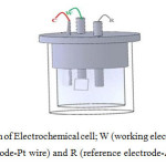 |
Figure1: Schematic diagram of Electrochemical cell; W (working electrode-Zn foil), C (counter electrode-Pt wire) and R (reference electrode-Ag/AgCl) Click here to View figure |
Characterization Details
Crystal structure and phase changes due to doping were characterized by X-ray diffraction (XRD, D8 Advance, BRUKER, Germany, Cu-Kα: λ=0.1540598 nm). Surface morphology examined by FE-SEM and elemental composition of doping element in the deposited films was obtained from EDAX. Resistivity measurements of the films are carried out by two point probe method. Surface height of film on the substrate is measured by using AFM (NanoSurf Easy Scan2, Switzerland). Absorption, Transmittance and Optical band gap curves of colloidal powder of films are obtained from Diffuse Reflectance UV-Vis spectrophotometer (JASCO V-670).
Resistivity Measurements
Resistivity of deposited films is measured by two probe technique. Film Thickness is measured by AFM and obtained as _ 1.5 μ m. Resistivity is calculated using below formula.
Resistivity (ρ) Ω-cm = [R*W*t] / L (1)
Where, ‘R’ is resistance obtained by two probes method, ‘W’ is contact width of probes,‘t’ is thickness of the film and ‘L’ is distance between probes.
Results and Discussion
Figure 2 shows the XRD patterns of pure and doped ZnO films of different compositions mentioned. Predominant peaks (100), (002) and (101) are observed in the range of ‘2θ’ values of
31.56° to 35.84°, which corresponds to hexagonal Wurtzite structure and there is no peak observed corresponding to secondary phase formation due to oxidization of Al. Lattice parameters of ‘a’= 3.282, ‘c’=5.26 and corresponding ‘c/a’ ratio of 1.602 closely matches with standard values of hexagonal structure. From the peaks, it can be observed that there is slight increase in the 2θ values, which corresponds to the decrease in‘d’ spacing of respective planes. Table 2 shows corresponding ‘2θ’ and‘d’ spacing values of pure and doped ZnO films.
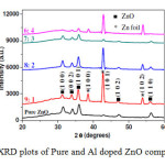 |
Figure2: XRD plots of Pure and Al doped ZnO compositions Click here to View figure |
The increase in ‘2θ’ values and decrease in‘d’ spacing values is due to incorporation of Al atom into crystal structure of ZnO, which can be in two ways: one is replacing Zn atoms and other is sitting in interstitial places of ZnO crystal structure. Al3+ ion in four coordination and has size of 54 pico meter which is less than size of Zn2+ ion size of 74 pico meter in the same coordination, which depicts that if Al replaces Zn atom in the structure, ‘d’ spacing of planes will decrease, which gives basic proof that Al is successfully doped into ZnO.
Table 2: Variation in ‘2θ’ and‘d’ spacing values for different molar ratios
|
Molar compositions (Zn nitrate: Al nitrate) |
2 Theta |
“d” spacing |
||
|
(100) |
(002) |
(100) |
(002) |
|
|
Pure ZnO |
31.491 |
34.160 |
2.83859 |
2.62268 |
|
9:1 |
31.256 |
33.921 |
2.85944 |
2.75584 |
|
8:2 |
31.379 |
34.031 |
2.84853 |
2.63230 |
|
7:3 |
31.431 |
34.073 |
2.84391 |
2.62919 |
|
6:4 |
31.341 |
34.089 |
2.85190 |
2.62795 |
From all the XRD plots, it is seen that (100) peak have high intensity which represents formation of flake-like structures of ZnO. Fig 3 shows an expanded view of XRD patterns showing only dominant peaks. From this figure, it is apparent that there is decrease in the intensity of peaks with increase in the content of Al, which could be due to decrease in the crystalinity of films [52]. From Table 2 it is observed that for the 6:4 composition there is reverse trend, i.e. increase in‘d’ spacing, which denotes that it is the saturation point of Al content for doping.
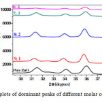 |
Figure3: XRD plots of dominant peaks of different molar compositions Click here to View figure |
Fig 4 shows Morphology characterization using FE-SEM for all compositions obtained. Mostly flake like structures are seen corresponding to formation of ZnO structures, which is in line with the dominant (101) peak observed in XRD results.
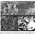 |
Figure4: FE-SEM images of Al-doped ZnO films deposited using different molar compositions Click here to View figure |
Elemental analysis (EDAX) is done to characterize the amount of Al content in the films deposited. Fig.5 shows the EDAX plots of all films of different compositions with contents of Al, O and Zn. Analysis is carried out at different regions of the films in order to obtain the minimum and maximum amounts of Al. Table 3 shows atomic percentage of Al, O2 and Zn contents at different regions.
Table 3: EDAX analysis data of Al, Zinc and oxygen contents with varying compositions
|
Composition (Zinc nitrate: Aluminium nitrate) |
At% of Zn |
At% of O2 |
At% of Al |
|||
|
Min |
Max |
Min |
Max |
Min |
Max |
|
|
9:1 |
62.61 |
79.30 |
19.22 |
36.23 |
1.16 |
2.38 |
|
8:2 |
42.69 |
47.85 |
51.47 |
55.40 |
0.68 |
1.91 |
|
7:3 |
40.52 |
40.53 |
56.46 |
57.17 |
2.3 |
3.02 |
|
6:4 |
37.57 |
43.29 |
54.09 |
57.49 |
2.62 |
4.98 |
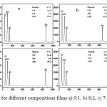 |
Figure5: EDAX for different compositions films a) 9:1, b) 8:2, c) 7:3 and d) 6:4Click here to View figure |
Al content in films of different compositions closely matches with the respective composition used for deposition of films, which supports the argument of Al doping. Resistivity measurements of the films are done using simple two probes resistivity method. From all above discussions, we can draw basic conclusion that Al is doped into the crystal structure of ZnO. If it is the case Al3+ ions which replaced Zn2+ atoms initiate in the electron flow in the films which decreases resistivity of films. Fig.6 shows plot of resistivity values with variation in the content of Al.
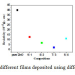 |
Figure6: Resistivity plot of different films deposited using different molar compositions |
As Al content is increased, resistivity decreases, which is in line with above discussions of doping Al into the crystal structure of ZnO, lowest resistivity is obtain for 7:3 composition i.e. 2.25×10⁻⁴ Ω cm. Increase in the resistivity for 6:4 composition is in accordance with the reversal of trends observed in XRD results, pointing to the saturation point of doping Al. All films are deposited on Zinc foil, so measurement of optical band gap and transmittance of the films is difficult, so the films are peeled off carefully from the substrate and are characterized by UV-VIS. Fig.7 (a) shows the plot of variation in the band gap for pure ZnO and 9:1 and 6:4 compositions films plotted using absorbance data of the powder and Fig.7 (b) shows the optical Transmittance of pure ZnO, 9:1 and 6:4 compositions.
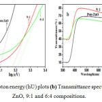 |
Figure7:(a) (αhƲ) 2 (vs) Photon energy (hƲ) plots (b) Transmittance spectra for compositions pure ZnO, 9:1 and 6:4 compositions.Click here to View figure |
From Fig.7 (a) it can be observed that there is a band gap widening with the variation in Al content in the deposited films, this is due to the second argument discussed in XRD section the Al ions can also sit in interstitial places of ZnO structure which increase the band gap of films. Transmittance plots plotted in the Fig.7 (b) shows the increase in the transmittance with doping which supports above discussion of band gap widening. Very good transmittance of 90% is obtained. From Transmittance graphs it can be seen that UV rays of wavelength below 300 can be blocked by using these films and as band gap engineering is possible with Al doping we can make use of these films for UV sensing devices.
Conclusion
Successful doping of Al into crystal structure of ZnO and improvisation of electrical property and optical property of the deposited films by the increase of Al content is reported by just simple and low temperature deposition by three electrode electro deposition techniques. XRD and EDAX details support the above argument of Al doping. We obtained low resistivity of 2.25 * 10-4 Ω cm for high doping composition of Al, obtained good optical transmission of 90% for doped ZnO which is more than that of pure ZnO. Optical band gap is also calculated using absorbance data and shows as there is as increase in composition of Al, the band gap is widening is observed. With all these results it can be concluded that deposited films show high conductivity, as well as high transmittance and with the opportunity of band gap engineering with varying Al content, these films will have potential usage in UV rays sensing devices.
References
- Byoungjun, P.; Kyoungah, C.; Sungsu, K.; Sangsig, K. P. Nanoscale Res Lett. 2011, 6, 41-45
- Panda, S. K.; Jacob, C. Solid-State Electronics. 2012, 73, 44-50
- Bo-Yuan, S.; Sheng-Yuan, C.; Yung-Der, J.; Mei-Chun, L.; Chia-Chiang, C.; Chin- Jyi, W. J. Electrochem. Soc. 2012, 159, 312-316
- Moe, K.; Wee, H. T.; Ghim, W. H. J. Mater. Chem. 2012, 22, 1644-1650
- Zhu, H.; Hupkes, J.; Bunte, E.; Huang, S. M. Chemphyschem. 2012, 13, 66-73
- Erin, L. R.; Ajaya, K. S.; Mariola, R. M.; Kenneth, N.; Paul, A.L.; David, S. G.; Neal, R. A.; Joseph, J. B. Thin Solid Film. 2012, 520, 5652–5663
- Ji-Zhou, K. F. Z.; Zheng, W.; Chuan-Bao, W.; Mei-Ling, W.; Kang-Min, C.; Xue-Mei, W.; Kong-Jun, Z.; Jin-Hao, Q. J Sol-Gel Sci Technol. 2012, 63, 95–102
- Jianzi, L.; Jian, X.; Qingbo, X.; Gang, F. Journal of Alloys and Compounds. 2012, 542, 151–156
- Ebrahimifard, R.; Abdizadeh, H.; Reza, M. G. Micro & Nano Letters. 2012, 7, 572-576
- Byeong-Yun, O.; Jeong-Hwan, K.; Jin-Woo, H.; Dae-Shik, S.; Hwan, S. J.; Ho-Jin, C.; Seong-Ho, B. K.; Jae, H. K.; Gi-Seok, H.; Tae-Won, K.; Kwang-Young, K. Current Applied Physics. 2012, 12, 273-279
- Dimopoulos, T.; Radnoczi, G. Z.; Horváth, Z. E.; Brückl, H. Thin Solid Films. 2012, 520,5222–5226
- Tarwal, N. L.; Devan, R. S.; Patil, R. S.; Karanjkard, M. M.; Patil, P.S. Electrochimica Acta. 2012, 72, 32– 39
- Sesha, V.; Amitha, S.; Dawson, P.; Karunakar, N.; Krupanidhi, S. B. Journal of Crystal Growth. 2012, 343, 7–12
- ElGhoul, J.; Barthou, C.; ElMir, L. Physica. 2012, 44, 1910–1915
- Necmettin, K.; Sadullah, O.; Lütfi, A.; Ahmet, A.; Zafer, Z. O. Journal of Alloys and Compounds. 2012, 536, 138–144
- Thongsuriwong, K.; Amornpitoksuk, P.; Suwanboon, S. J Sol-Gel Sci Technol, 2012, 62, 304–312
- Zheng, J. H.; Song, J. L.; Jiang, Q.; Lian, J. S. J Mater Sci Mater Electron. 2012, 23, 1521–1526
- Vishwas, M.; Narasimha, K. R.; Arjuna, K. V. G.; Chakradhar, R. P. S. Spectrochimica Acta Part A: Molecular and Biomolecular Spectroscopy. 2012, 95, 423–426
- Jun, B. Z.; Jian, Z. L.; Xi, Y. H.; Jun, Z.; Yan, L.; Wei, H.; Kun, L. Current Applied Physics. 2012, 12, 998-1001
- Mansoor, A.; Seyyed, E. M. F. Journal of Rare Earths. 2012, 30, 38-38
- Shuangxue, Z.; Ping, L.; Yu, W. Powder Technology. 2012, 224, 390-394
- Yang, H.; Xu, X.; Zhang, G.; Miao, J.; Zhang, X.; Wu, S.; Jiang, Y. Rare Metals. 2012, 31, 154-156
- Ton-Thata, C.; Matthew, F.; Matthew, R. P.; Takuya, T.; Zoe, S. Journal of Alloys and Compounds. 2012, 522, 114-117
- Qiang, S.; Junying, Z.; Dong, Z.; Changzheng, W.; Bing, Y.; Bingyuan, Z.; Wenjun, W. Materials Science and Engineering B. 2012, 177, 689-693
- Pradipta, K. N.; Caraveo-Frescas, J. A.; Unnat, S. B.; Alshareef, H. N. Appl. Phys. Lett. 2012, 100, 253507-253511
- Lingyun, Z.; Yulin, Y.; Ruiqing, F.; Haiyan, C.; Ruokun, J.; Yonghui, W.; Liqun, M.; Yazhen, W. Materials Science and Engineering B. 2012, 177, 956-961
- Díez-Betriu, X., Jiménez-Rioboo, R., Sánchez- Marcos, J., Céspedes, E., Espinosa, A., Andrés, A. Journal of Alloys and Compounds. 2012, 536, 592-598
- Meiqin, Z.; Gang, Q.; Yueping, Z.; Ting, Z.; Yang, Z.; Lei, S.; Hong, Q.; Xueji, Z. Electrochimica Acta. 2012, 78, 412-416
- Zhou, H. B.; Zhang, H. Y.; Wang, Z. G.; Tan, M. L. Materials Letters. 2012, 74, 96-99
- Naoki, T.; Nobuto, O.; Yuzo, S. Thin Solid Films. 2012, 520, 3751-3754
- Jianfeng, S.; Chunjuan, T.; Qiang, N.; Chunhe, Z.; Yongsheng, Z.; Zhuxi, F. Applied Surface Science. 2012, 258, 8595-8598
- Zhu, B. L.; Wang, J.; Zhu, S. J.; Wu, J.; Zeng, D. W. Xie, C. S. Thin Solid Films. 2012, 520, 6963-6969
- Jianzi, L.; Jian, X.; Qingbo, X.; Gang, F. Journal of Alloys and Compounds. 2012, 542, 151-156
- Hirahara, N.; Onwona-Agyeman.; Nakao, M. Thin Solid Films. 2012, 520, 2123-2127
- Pham, H.Q.; Ngo-Dinh, S.; Do-Quang, N. Thin Solid Films. 2012, 520,6455–6458
- Wonkyun, Y.; Junghoon, J. Current Applied Physics. 2012, 1, 5-12
- Crossay, A.; Buecheler, S.; Kranz, L.; Perrenou, J.; Fell, C. M.; Romanyuk, Y. E.; Tiwari, A. N. Solar Energy Materials & Solar Cells. 2012, 101, 283-288
- Mingsong, W.; Weiqiang, L.; Yunfeng, Y.; Juan, Y.; Xiaonong, C.; Sung, H. H.; Eui, J. K. Materials Chemistry and Physics. 2012, 134, 845-850
- Sanghwa, Y.; Ilgoo, H.; Jae-Hong, L.; Bongyoung, Y. Current Applied Physics. 2012, 12, 784-788
- Kishwar, S.; Hasan, K.; Alvi, N. H.; Klason, P.; Nur, O.; Willander, M. Superlattices and Microstructures. 2011, 49, 32-42
- Lupan, O.; Pauporte, T.; Chow, L.; Viana, B.; Pelle, F.; Ono, L. K.; Roldan, B. C.; Heinrich, H. Applied Surface Science. 2010, 256, 1895-1907
- Bjoern, S.; Athavan, N.; Ben, W.; Rolf, K. Materials Letters. 2009, 63, 736-738
- Yiwen, T.; Lijuan, L.; Zhigang, C.; Yun, J.; Bihui, L.; Zhiyong, J.; Liang, X. Electrochemistry Communications. 2007, 9, 289-292
- Ramırez, D.; Silva, D.; Gomez, H.; Riveros, G.; Marotti, R. E.; Dalchiele, E. A. Solar Energy Materials & Solar Cells. 2007, 91, 1458-1461
- Dalchiele, E. A.; Giorgi, P.; Marotti, R. E.; Martın, F.; Ramos-Barrado, J. R.; Ayouci, R.; Leinen, D. Solar Energy Materials & Solar Cells. 2001, 70, 245-254
- Chunfu, L.; Hong, L.; Jianbao, L.; Xin, L. Journal of Alloys and Compounds. 2008, 462, 175-180
- Wellings, J. S.; Chaure, N. B.; Heavens, S. N.; Dharmadas, I. M. Thin Solid Films. 2008, 516, 3893-3898
- Hosang, A.; Yaqi, W.; Seung, H. J.; Minseo, P.; Young, S. Y.; Dong-Joo, K. Chemical Physics Letters. 2011, 511, 331-335
- Yi-Jing, L.; Kun-Mu, L.; Chiu-Yen, W.; Chung, K.; Lih-Juann, C. Sensors and Actuators B. 2012, 161, 734-739
- Marı, B.; Manjon, F. J.; Mollar, M.; Cembrero, J., Gomez, R., (2006) Applied Surface Science. 2006, 252, 2826-2831
- Jaeyoung, L.; Yongsug, T. Electrochemistry Communications, 2000, 22, 765–768
- Tortosa, M.; Manjon, F. J.; Mollar, M.; Marı, B. Journal of Physics and Chemistry of Solids. 2012, 73, 1111-1115
- Asish, B. M.; Pavan, K. Y. International Journal of Advanced Research in Engineering & Technology. 2013, 4, 46 – 55
- Meena, A. S.; Meena, P. L.; Chandra, M.; Meena, R.; Shribai, Meena, R. C. International Journal of Electrical Engineering & Technology. 2013, 4, 180-187
- Prachi, S.; Navneet, G. International Journal of Electronics and Communication Engineering & Technology, 2013, 4, 115 – 127

This work is licensed under a Creative Commons Attribution 4.0 International License.


