Preparation and Characterization of Indium and Gallium doped Transparent ZnO Films for Solar Cell Applications
Reuben Seth Richter1,3, A. Yaya1, D. Dodoo-Arhin1,3, B. Agyei-Tuffour1, Robinson Juma Musembi2,3 and Boateng Onwona-Agyeman1,3
1Department of Materials Science and Engineering, University of Ghana, Legon, Accra, Ghana.
2Department of Physics, University of Nairobi, Nairobi, Kenya.
3African Materials Science and Engineering Network, AMSEN, A Carnegie – IAS RISE Network.
Corresponding Author E-mail: BOnwona-Agyeman@ug.edu.gh
DOI : http://dx.doi.org/10.13005/ojc/340513
Article Received on : 13-07-2018
Article Accepted on : 30-08-2018
Article Published : 12 Oct 2018
In this work, the effect of indium (In) and gallium (Ga) dopants on the structural, optical and electrical properties of ZnO thin films was studied. ZnO thin films were deposited on glass substrates at 400°C using the spray pyrolysis deposition technique. X-ray diffraction (XRD) results indicated that both undoped and doped ZnO films had (002) preferred orientation. The undoped ZnO films were found to exhibit high transmittance above 80%, while indium-doped (In:ZnO) and gallium-doped (Ga:ZnO) films had transmittance above 60% and 70% respectively. From the Hall Effect measurements, doping improved the conductivity of the ZnO thin films however, In:ZnO films showed higher electrical conductivity compared to Ga:ZnO films. Electron probe microanalysis (EPMA) results were used to confirm the presence of the respective dopants in the thin film samples.
KEYWORDS:Crystal Structure; Spray Pyrolysis; Sheet Resistance; Thin Films; Transparent Semiconductors
Download this article as:| Copy the following to cite this article: Richter R. S, Yaya A, Dodoo-Arhin D, Agyei-Tuffour B, Musembi R. J, Onwona-Agyeman B. Preparation and Characterization of Indium and Gallium doped Transparent ZnO Films for Solar Cell Applications. Orient J Chem 2018;34(5). |
| Copy the following to cite this URL: Richter R. S, Yaya A, Dodoo-Arhin D, Agyei-Tuffour B, Musembi R. J, Onwona-Agyeman B. Preparation and Characterization of Indium and Gallium doped Transparent ZnO Films for Solar Cell Applications. Orient J Chem 2018;34(5). Available from: http://www.orientjchem.org/?p=50654 |
Introduction
Solar cells consist of various materials, each performing a specific function which contributes to the overall efficiency of the solar cell. The Transparent Conducting Oxide/Film (TCO) is an important component of the solar cell design. This component is responsible for the collection and transporting electrons generated after the photoexcitation process. It is required that, the TCO be optically transparent and electrically conductive. TCOs are also used in other electro-op devices such as light emitting diodes (LED) touch and flat panel displays.1,2 Various materials have been used as TCO in solar cells including tin doped indium oxide (ITO), fluorine-doped tin oxide (FTO) and indium-doped cadmium oxide (In : CdO). The above-mentioned materials have disadvantages such as high cost, toxicity and unavailability. An alternative TCO material is Zinc oxide (ZnO). Zinc oxide is a wide-band-gap semiconductor with a direct band gap of 3.3 eV at room temperature.3 The wide band gap makes zinc oxide transparent to light with high transmittance. The lattice parameters ‘a’ and ‘c’ of ZnO which has a wurtzite crystalline structure are 3.24 Ȧ and 5.19 Ȧ respectively.4,5 The undoped ZnO has a very low electrical conductivity and hence requires doping to improve the conductivity. Factors that influence the choice of dopants include valency, electronegativity and ionic radius. Some of the common dopants used to improve conductivity of ZnO are aluminum and fluorine. Eventhough much work has been done to study the effects of these dopants on ZnO, there still remains some gaps in understanding the behaviour of these dopants.6-9
There are several thin film deposition techniques employed in the fabrication of TCOs.10-13 These deposition systems can be classified physical vapor deposition (PVD), chemical vapor deposition (CVD) and solution growth. Most PVD and CVD techniques require complex equipment setup and operate under low pressure or high vacuum conditions. This makes these techniques very expensive. An alternative technique which has a relatively simple setup, operates in atmospheric conditions and can be scaled up easily is spray pyrolysis. Spray pyrolysis has been used to grow ZnO films with very good structural, optical and electrical properties.14
In this work, indium doped ZnO and gallium doped ZnO thin films are prepared by spray pyrolysis and characterized to determine their optical, electrical and structural properties.
Materials and Method
The undoped ZnO, In-doped ZnO and Ga-doped ZnO thin films were deposited on soda lime glass substrates using spray pyrolysis. The glass substrates were washed in an ultrasonic cleaner for half an hour using separate solutions of ethanol (95%), acetone and distilled water. After cleaning, the glass substrates were preheated at a temperature of 400°C to remove any traces of impurities that may be present even after cleaning. 0.2M aqueous solutions of Zinc acetate (99.9% – Sigma Aldrich) were used as the precursor solution for the deposition process. The sources of indium and gallium dopants were indium (III) chloride and gallium oxide respectively and the doped ZnO films were prepared by mixing known concentration of aqueous solutions of indium (III) chloride and gallium oxide to the zinc acetate solution. The films were deposited at a temperature of 400° in a non-vacuum environment. The transmittance of the films was measured using a Genesys 10S UV-Vis spectrophotometer. The parameters used were a minimum wavelength of 350nm, with scan interval 15nm and a maximum wavelength of 800nm.
The surface morphology of the films were studied using a field emission gun scanning electron microscope (FEG-SEM), JEOL 5800 and operating in the secondary mode.
The XRD analysis was performed using a scan axis of 2θ from 20.00 to 80.00°. A step size of 0.2 was also programmed. The anode material for the X-ray diffractometer was Cu with Kα radiation of wavelength 0.154 nm.
Hall Effect Measurements was carried out on doped zinc oxide thin films. The doped samples were subjected to a magnetic field with electric current passing through the magnetic field in a perpendicular direction. Molten lead was deposited at the four corners of the sample and allowed to solidify to form contacts. Thin wires were embedded in the lead contacts and these served as ports for the probes. The experiment was carried out at a temperature of 300K (27°C). For the purposes of this experiment, a magnetic field of 300mT was created by supplying current to a pair of electromagnets. The magnetic strength was measured with a Phywe Teslameter. For each sample (In:ZnO 1wt% -5wt% / Ga:ZnO 1wt% -5wt%), a minimum current of -10mA (reverse current) was applied. The current was varied by a step size of 1mA up to a maximum of 10mA. At each current, the corresponding voltage created was recorded using a digital multimeter. Voltage correction was done based on the voltages recorded at 0mA for each sample to attain the actual Hall voltages (VH). A plot of the input current against the Hall voltage was generated and the slope of the graph used to determine the Hall coefficient.
Electron Probe Microanalysis (EPMA) using JEOL 5800 was carried out on In:ZnO and Ga:ZnO samples to ascertain the presence of the intended dopants and other elements in the ZnO structure. The analysis also gave further information about the relative concentration of these elements.
Results and Discussions
Optical transmittance
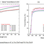 |
Figure 1: Optical transmittance of; a) In:ZnO and b) Ga:ZnO. |
The aim of carrying out this characterization was to find out how much light the TCO transmits and absorbs within the ultraviolet and visible range of the electromagnetic spectrum (EMS). For the In:ZnO samples, the optical transmittance increased steadily until a concentration of 5wt% sample where there was a drop (Fig.1a). The increase in optical transmittance for the In:ZnO may be attributed to good crystal properties. As the crystallinity of the ZnO structure improves, less scattering of light occurs and the transmittance values increase. The average optical transmittance of the In:ZnO was above 60% with the 4wt% In:ZnO sample recording the highest average transmittance value of 72.98%. For the Ga:ZnO thin films, there was a steady decrease in the transparency of the films as the dopant concentration was increased as shown in Figure 1b. This will cause high light scattering that will affect the transmittance values. The drop in transmittance may be due to the homogeneity of the precursor solution. As the dopant concentration was increased, incomplete dissolution of the dopant compounds in the precursor solution could have affected the film formation process during the deposition.16,17 The 1wt% Ga:ZnO sample recorded the highest average transparency (87.56%).
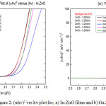 |
Figure 2: (αhv)2 vrs hv plot for; a) In:ZnO films and b) Ga:ZnO.
|
The band gap for the doped samples was obtained by extrapolating the linear portion of the Tauc plot of (αhν)2 against hν as shown in Figure 2. The band gap in eV is the intercept of the extrapolated line on the x-axis. The undoped ZnO samples had an average band gap of 3.25eV. In Figure 2a, the band gap of 1wt% In:ZnO and 2wt% were 3.125 and 3.129eV respectively. The Ga:ZnO films recorded an average of 3.25eV as is in Figure 2b. Comparing the band gap values for the undoped ZnO, In:ZnO and Ga:ZnO, it could be suggested that, the reduction in resistivity of the In:ZnO can be attributed to the narrowing of the band gap.18,19 Also, the band gap of Ga:ZnO did not change significantly from the undoped ZnO hence the effect of the gallium dopant in reducing the resistivity was not as significant as In:ZnO.
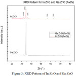 |
Figure 3: XRD Pattern of In:ZnO and Ga:ZnO. |
The X-ray diffraction analysis was used to study the crystal structure of the doped zinc oxide samples and determine if a peak shift occurred because of the doping of ZnO. Figure 3 shows the X-ray diffraction pattern for the doped ZnO thin films. The XRD diffraction peaks occurring at 2θ=31.09, 34.54, 36.34, 56.63 and 62.94 correspond to the (100), (002), (101), (110), (103), planes of the hexagonal structure of the doped ZnO analyzed. The most dominant peak for both 1wt% – indium doped zinc oxide (In:ZnO) and gallium doped zinc oxide (Ga:ZnO) was the (002) peak. However, the (002) peak of the Ga:ZnO sample had higher intensity as compared to the In:ZnO sample. The peak for the preferred (002) orientation occurred at 34.414° and 34.422° for In:ZnO and Ga:ZnO respectively as expected.14 From this data, it can be said that, there was no peak shift after doping ZnO with indium and Gallium. Other less dominant peaks that showed on the XRD pattern for the In:ZnO sample were (100), (101), (110) and (103). This can be attributed to the difference in atomic radii of indium and zinc.20 Indium has a larger atomic radius (1.56Å) compared to zinc (1.42Å). The difference in atomic radius causes stress in the ZnO structure when indium replaces zinc. This is seen in the various peaks except that of the preferred (002) orientation in the In:ZnO sample. Gallium however has a smaller atomic radius (1.36Å) compared to zinc and indium. From Figure 5, it is observed that, the (002) orientation from Ga:ZnO is most dominant and the other peaks have less intensities when compared. The smaller atomic radius of gallium allows it fit with less strain on the zinc oxide structure as compared to indium. This therefore explains the difference in peak intensities for the (002) peaks and the appearance of other peaks and corresponding low intensities for both samples.
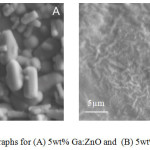 |
Figure 4: SEM micrographs for (A) 5wt% Ga:ZnO and (B) 5wt% In:ZnO (x5000). Click here to View figure |
The surface morphology of In:ZnO and Ga:ZnO doped films made up of 5wt % were studied using the scanning electron microscope (see Figure 4). In Figures 4A and 4B, it is evident that, there is a distinct variation in the surface morphology of In:ZnO and Ga:ZnO doped films. Ga:ZnO (Fig. 4A), had cylindrical rod-shaped crystallites while that of In:ZnO (Fig. 4B), had characteristic hexagonal slices. These plate-like structures spread across the surface fused together and overlapping to give a rough surface. The Ga:ZnO crystallites however were clustered in pockets with varying diameters. The difference in crystallite structure and distribution serves as an explanation for the different optical transparency values recorded.
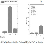 |
Figure 5: EPMA chart of a) In:ZnO and b) Ga:ZnO at 5wt%.
|
The values obtained from the EPMA analysis are graphically represented in Figures 5 (a & b). It can be inferred from the plot in Figure 5a for In:ZnO that, indium was present in the doped zinc oxide sample. The improvement in the conductivity of these samples can be attributed to the presence on indium. The amount of indium (mass %) in the 5wt% sample was 9.112. Similarly, the presence of gallium was detected in the Ga:ZnO samples (Figure 5b) and hence improvement in the conductivity of the respective samples can be attributed to the presence of gallium. Also, the amount (mass%) of gallium in the 5wt% sample was 4.303. The other trace elements such as silicon and boron that were observed in all samples (both In:ZnO and Ga:ZnO) could be from the glass substrate the carried the thin film. Also, chlorine and calcium in both In:ZnO and Ga:ZnO respectively, were from the dopant source compounds. The indium dopant was sourced from indium (III) chloride while gallium was sourced from gallium oxide. The analysis therefore confirmed the presence of both dopants in the respective samples and the deductions made with respect to the electrical properties of doped ZnO samples.
Hall Effect Measurements
Tables 1 and 2 summarizes the sheet resistance, mobility and carrier concentration of the In:ZnO and Ga:ZnO thin film samples prepared. For the In:ZnO, the sheet resistance decreases with increasing dopant concentration. The lowest sheet resistance and the highest mobility were obtained when the ZnO was doped with 1wt% In. The sheet resistance of the Ga:ZnO were all in the mega ohm range and as explained earlier maybe due to the ionic radius of Ga 3+ which is larger than the In3+. These metallic dopants replace Zn2+ in the crystal structure of ZnO and therefore the size of the dopant also determines the electrical properties of the semiconductor. These results from the Hall Effect measurements and the UV-Visible spectrophotometer indicate the potential use of these doped-ZnO films as TCOs normally used in solar cell applications.
Table 1: Electrical properties of In:ZnO.
|
In:ZnO |
||||
| Dopantconcentration.(wt%) | Sheetresistance(kΩ) | Mobility(cm2/Vs) | Carrierconcentration(cm-3) | |
| 1 | 98.28 | 2.43 x 10⁻⁴ | 3.48 x 10²¹ | |
| 2 | 115.78 | 2.13 x 10⁻⁴ | 3.38 x 10²¹ | |
| 3 | 156.97 | 1.60 x 10⁻⁴ | 3.33 x 10²¹ | |
| 4 | 190.44 | 1.41 x 10⁻⁴ | 3.11 x 10²¹ | |
| 5 | 260.81 | 1.17 x 10⁻⁴ | 2.74 x 10²¹ | |
Table 2: Electrical properties of Ga:ZnO.
|
Ga:ZnO |
|||
| Dopantconcentration.(wt%) | Sheetresistance(MΩ) | Mobility(cm2/Vs) | Carrierconcentration(cm-3) |
| 1 | 6.60 | 4.24 x 10⁻⁶ | 2.98 x 10²¹ |
| 2 | 6.51 | 4.31 x 10⁻⁶ | 2.97 x 10²¹ |
| 3 | 8.90 | 3.15 x 10⁻⁶ | 2.97 x 10²¹ |
| 4 | 13.12 | 2.14 x 10⁻⁶ | 2.97 x 10²¹ |
| 5 | 20.96 | 1.34 x 10⁻⁶ | 2.96 x 10²¹ |
Conclusions
UV-Vis spectroscopy, Hall Effect, X-ray diffraction, and EPMA analysis were carried out on the undoped and doped ZnO thin films prepared by spray pyrolysis technique.
UV-Vis spectrophotometry analysis showed that the In:ZnO thin films had transparency above 60% and the transparency increased with increasing dopant concentration. For the Ga:ZnO thin films, a maximum transparency of 88% was recorded for the 1wt% sample. From the Hall Effect measurement and sheet resistance analysis, the conductivity, electron mobility and carrier concentration decreased with increasing dopant concentration. The In:ZnO samples however exhibited higher conductivities, mobility and charge concentration compared to the Ga:ZnO.
The X-ray diffraction results revealed that both In:ZnO and Ga:ZnO thin films were highly oriented with dominant (002) peaks.
Electron probe microanalysis results showed that, both indium and gallium were present in their respective doped films. The composition of indium in mass percent for both In:ZnO samples was higher than that of gallium in the respective Ga:ZnO samples. This indicated that, more indium dopant had been successfully incorporated in the ZnO during the spray pyrolysis process. Based on the results obtained from the doped samples both doped thin films can be used TCOs in opto-electronic devices such as solar cells.
Acknowledgements
The authors would like to acknowledge the financial and technical support of AMSEN*. The following also provided technical support for the work:
Modern Physics laboratory, Physics Department, University of Cape Coast, Ghana.
Electronics laboratory, Physics Department, University of Ghana, Ghana.
References
- Stadler, Andreas (2012), Transparent Conducting Oxides – An Up-To-Date Overview, MDPI Materials Journal (5), 661- 683.
- B. Godbole, N. Badera, S. Shrivastava, D. Jain, V. Ganesan (2011), Growth Mechanism of ZnO Films Deposited by Spray Pyrolysis Technique, Materials Sciences and Applications, 2, 643 – 648.
CrossRef
- M. Krunks, E. Mellikov (1995), Zinc oxide thin films by the spray pyrolysis method, Thin Solid Films (270), 33-36.
CrossRef
- X. Lou (1991), Development of ZnO series ceramic semiconductor gas sensors. J. Sens. Trans. Technol., 3, 1-5.
- F. Paraguay D., W. Estrada L., D.R. Acosta N., E. Andrade, M. Miki-Yoshida (1999), Growth, structure and optical characterization of high quality ZnO thin films obtained by spray pyrolysis. Thin Solid Films(350), 192-202.
CrossRef - F.Z. Bedia, A. Bedia, M. Aillerie, N. Maloufi, F. Genty and B. Benyoucef, (2014), Al-doped Zno transparent contacts deposited by a spray pyrolysis technique on performance of HIT solar cells. Energy Procedia(50), 853-861.
CrossRef - J.N. Ding, C.B. Tan, N.Y. Yuan, X.W. Feng, X.Y. Chang, F. Ye. 2012. The preparation and properties of Al-doped ZnO thin films as transparent electrodes for solar cell. Physics Procedia (32): 789-794.
CrossRef
- A. Crossay, S. Buecheler, L. Kranz, J. Perrenoud, C.M. Fella, Y.E. Romanyuk , A.N. Tiwari. 2012. Spray-deposited Al-doped ZnO transparent contacts for CdTe solar cells. Solar Energy Materials & Solar Cells 283-288.
CrossRef
- P.M. Ratheesh Kumar, C. Sudha Kartha, K.P. Vijayakumar, F. Singh, D.K. Avasthi. 2005. Effect of fluorine doping on structural, electrical and optical. Materials Science and Engineering (B 117): 307-312.
- R.H. Horng, D.S. Wuu, Y.C. Lien, W.H. Lan. (1999), Low-resistance and high-transparency Ni/indium tin oxide ohmic contacts to p-type GaN. Applied Physics Letters 79.
- R. Groenen, J. Loffler, P.M. Sommeling, J.L. Linden, E.A.G. Hamers, R.E.I. Schropp, M.C.M. van de Sanden, (2001), Surface textured ZnO films for thin film solar cell applications by expanding thermal plasma CVD. Thin Solid Films, 392, 226 – 230.
CrossRef - R. Biswal, A. Maldonado, J. Vega-Pérez , D. R. Acosta and M. De La Luz Olvera, (2014), Indium doped zinc oxide thin films deposited by ultrasonic chemical spray technique, starting from zinc acetylacetonate and indium chloride. Materials journals, 5038-5046.
- N. Hirahara, B. Onwona-Agyeman and M. Nakao (2012), Preparation of aluminum-doped ZnO as transparent conductive substrate in dye-sensitized solar ell. Thin Solid Films, 520 (6), 2123-2127.
CrossRef - F. Yakuphanoglu,Y. Çağlar, S. Ilican, M. Caglar, (2007), The effects of fluorine on the structural, surface morphology and optical properties of ZnO thin films, Physica B (394), 86-92
CrossRef
- R. Biswal, L. Castaneda, R. Moctezuma, J. Vega-Perez, M. De La Luz Olvera and A. Maldonado, (2012), Formation of Indium-Doped Zinc Oxide Thin Films Using Ultrasonic Spray Pyrolysis: The importance of the Water Content in the Aerosol Solution and the Substrate Temperature for Enhancing Electrical Transport. MDPI Materials Journal, 5, 432 – 44.
CrossRef - P. V. Raghavendra and J. S. Bhat (2017), Optical properties of strontium doped zinc oxide thin films: AIP Conference Proceedings 1832, 080067.
- H. Rotella, Y. Mazel, S. Brochen, A. Valla, A. Pautrat, C. Licitra, N. Rochat, C. Sabbione, G. Rodriguez and E. Nolot (2017), Role of vacancy defects in Al doped ZnO thin films for optoelectronic devices: J. Phys. D: Appl. Phys. 50, 485106.
- K. Ellmer, A. Klein and B. Rech, (2007), Transparent Conductive Zinc Oxide (Springer Series in Materials Science vol 104) (Berlin: Springer) (https://doi.org/10.1007/978-3-540-73612-7)
- I. Hamberg and C.G. Granqvist (1986), Evaporated Sn-doped In2O3 films: Basic optical properties and applications to energy-efficient windows: J. Appl. Phys. 60, 23–60.
CrossRef
- Q.J. Wang , J.B. Wang , X.L. Zhong , Q.H. Tan , Z. Hu and Y.C. Zhou (2012), Magnetism mechanism in ZnO and ZnO doped with nonmagnetic elements X (X = Li, Mg, and Al): a first-principles study: Appl. Phys. Lett. 100, 132407.
CrossRef

This work is licensed under a Creative Commons Attribution 4.0 International License.


